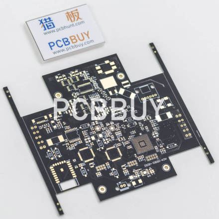
What Is Immersion Gold Pcb?(4 Answers)
By: 05/31/2023 16:00
Electroless gold plating and gold immersion plating are commonly used processes in circuit board production nowadays. In simple terms, electroless gold plating involves the chemical deposition of a layer of metal coating on the surface of the circuit board through a chemical oxidation-reduction reaction.
The copper on the circuit board is mainly made of pure copper, which is susceptible to oxidation in the air. This can lead to poor solderability or inadequate contact, thereby reducing the performance of the circuit board.
As a PCB manufacturer specializing in high-end applications, PCBBUY has provided customized services to multiple well-known companies.
If you want to order PCB product, please check and custom your order online.
Why is Immersion Gold Pcb used?
The copper on the circuit board is mainly made of pure copper, which is susceptible to oxidation in the air. This can lead to poor solderability or inadequate contact, thereby reducing the performance of the circuit board.
To address this issue, surface treatment is required for the copper solder joints. Electroless gold plating is a process that deposits a layer of gold on the surface, effectively acting as a barrier between the copper metal and the air to prevent oxidation. Therefore, electroless gold plating is a method of surface oxidation prevention, where a layer of gold is chemically deposited on the surface of the copper, also known as gold immersion.
What are the characteristics of Immersion Gold PCB?
l The gold-plated board has a bright color, good appearance, and attractive visual appeal.
l The crystalline structure formed by electroless gold plating enables better soldering performance, ensuring quality.
l Since the gold plating is only present on the solder pads, it does not affect the signal transmission on the copper layer due to the skin effect.
l Gold has stable metallic properties and a denser crystal structure, making it less susceptible to oxidation reactions.
l As only the solder pads have nickel-gold plating in electroless gold PCBs, the bond between the solder mask and the copper layer is stronger, reducing the chances of micro-shorting.
l Engineering compensation does not affect the spacing of the circuit.
l The stress in electroless gold-plated boards is easier to control.
What are the benefits of Immersion Gold plating as a surface treatment?
The advantages of electroless gold plating include stable color deposition, excellent brightness, and a smooth and even coating, resulting in excellent solderability.
Typically, the thickness of gold in electroless gold plating is around 1-3 microns, making it relatively thicker compared to other surface treatment methods. This makes electroless gold plating commonly used in applications such as keypad boards and gold finger boards, as gold has strong conductivity, good oxidation resistance, and a long service life.
What are the advantages of using a circuit board with Immersion Gold plating?
l The gold-plated board has a bright color, good appearance, and attractive visual appeal.
l The crystalline structure formed by electroless gold plating enables better soldering performance, ensuring quality.
l Since the gold plating is only present on the solder pads, it does not affect the signal transmission on the copper layer due to the skin effect.
l Gold has stable metallic properties and a denser crystal structure, making it less susceptible to oxidation reactions.
l As only the solder pads have nickel-gold plating in electroless gold-plated boards, the bond between the solder mask and the copper layer is stronger, reducing the chances of micro-shorting.
l Engineering compensation does not affect the spacing of the circuit.
l The stress in electroless gold-plated boards is easier to control.
Customized processes with PCBBUY:
l Support for 1-14 layer small to medium batch orders; for more layers, consult customer service.
l HDI blind via technology is available.
l The board material uses JianTao A-level board (KB-6164) and can be made halogen-free.
l Maximum size can be up to one meter.
l Various ink colors such as pink, transparent, and purple are available.
l Support for copper thickness up to 10oz and hole copper of 35μm.
l Customizable lamination structure for multilayer boards.
l Support for multi-level impedance matching.
l Special processes such as copper wrap around the board edge, dual-tone ink, press-fit holes, counterbore holes, slots, stepped holes, stepped slots, and selective nickel-palladium-gold plating are available.
l PCBA assembly starting from one set, available for single or double-sided assembly.
Industry Category


