
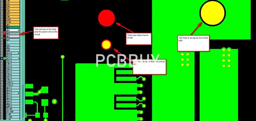
All the holes as big as the circuit pads, the circuit pads smaller than the holes, the holes without the circuit pads, and the holes without electrical performance connections (no grounding wire and copper). We will make all of them according to NPTH hole and ignore the hole pattern and other requirements for such holes.
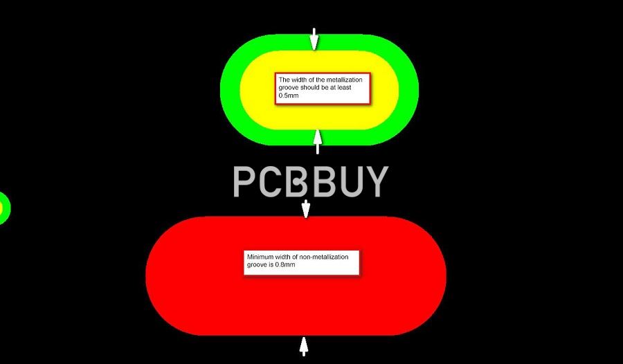
The minimum non-metallization groove made by our company is 0.8mm, the minimum metallization groove is 0.5mm (referring to the original design size),if less than this specification, we will take the center of the groove as the standard, to both sides of the increase to 0.8mm or 0.5mm production, only add width without length.
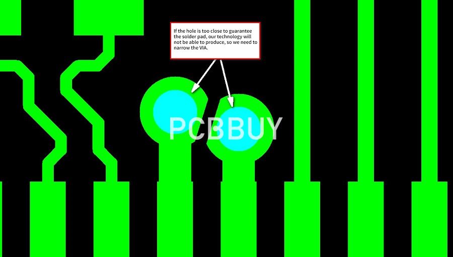
If there are individual electrical holes with copper VIA through holes (VIA holes are only used for electrical conductivity, not Press Fit Hole), our process cannot be processed due to too small spacing and cannot be moved, we can reduce such holes by ourselves within 0.1mm.
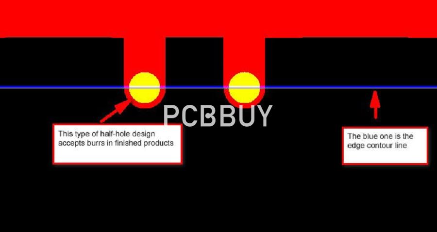
For the boards with half-hole design, please accept the copper burr in the finished holes and slight copper pulling at the edge of the half-hole plate. Because our company's production process is to be unified, we cannot produce separately according to the special half-hole process. For our half-hole processing, the minimum hole shall be 1.0mm and the single small board shall not be more than 5.
On one side the circuit pad is very big, and the other side there is no pad, there is enough space in the PCB file under the condition of production, we are all according to the default according to PTH hole is made, If there is enough space to manufacture according to the PCB file, we will produce the PTH hole by default. To ensure that we can process would be able to produce, We will directly add a circuit pad 0.127mm larger than the hole on the side where there is no circuit pad, and the little pad will dew on the copper surface process, However, please note that if such holes are designed in the GKO layer or GM1 layer in the document, we will make them according to the NPTH hole in this case.
The whole board of bare copper must have a surface process (such as immersion gold and HASL), so our company cannot produce it separately according to this single type of board without a surface process.

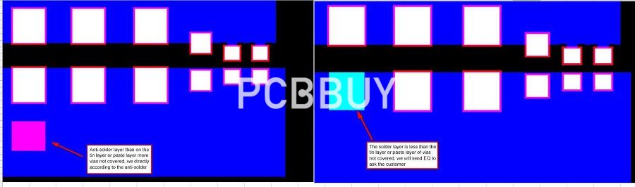
If there is a conflict between solder layer and tin layer and paste layer, if the solder layer opens more vias not covered than tin layer and paste layer, we will directly make the solder layer (please pay attention to the omission of solder vias not covered when updating and upgrading). When the anti-solder layer is less than the tin layer, we will ask your company questions in EQ.
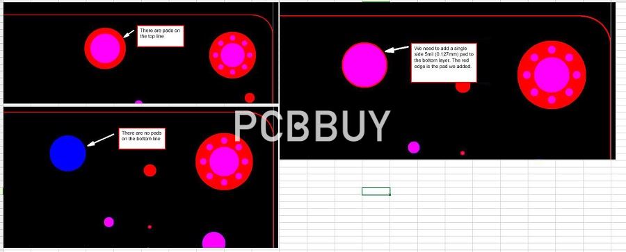
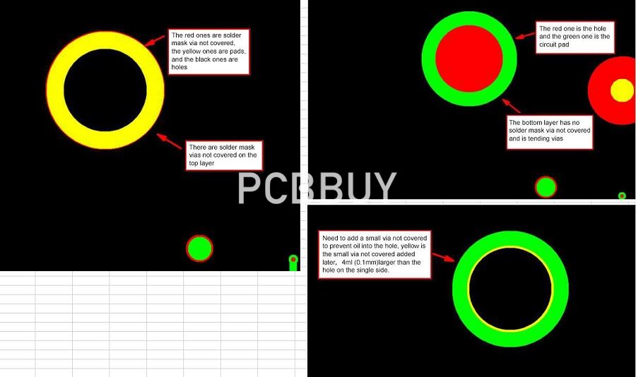
The corresponding plug-in PTH hole vias not covered, one side has a via not covered, and the other side has no via not covered, in order to ensure that the ink does not enter the hole, We need to add a single side welding oil stop 0.1mm larger than the hole on the side without via not covered, the finished hole edge will have exposed copper on the surface of the phenomenon.
For the data of AD series, Protel series and other designs, we will all tending vias, PADS, Gerber and other forms of documents for the VIA processing method. For the VIA processing method, we will design according to the file, tending vias or vias not covered. We will ignore the requirements in PCB board, and special requirements need to be noted out.
Requirement of ink plug hole board, in the absence of special remarks of a certain plugged vias, we will be according to the green light cannot transparent white light of the ordinary plug hole requirements to make.
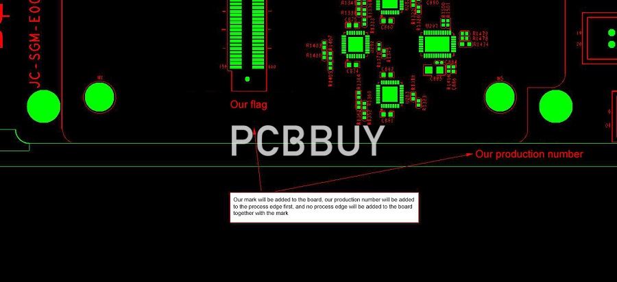
silk screen layer will be added our mark and our production number, tag, in a single small plates with number priority to add on the edge of the process, would we be without technology edge with tags within the board, so convenient you I identified the two recognition (no silk screen layer and isn't there room in the veneer we won't add any tag, Text layer not mark up the special remarks) or even your company, please provide the production before the file will be default is allowed to add our internal identify factory of (our internal recognition factory is not necessarily the same as the ship model, it is an identification number, either as our factory logo, also can prevent the internal mixing board).Otherwise, even if the files provided by your company are previously produced, we will be considered to add the internal identification of our company by default (Our company's internal identification number may be not the same as the shipped model. It is just an identification number, which can be used as our company's factory identification and can also prevent internal confusion)
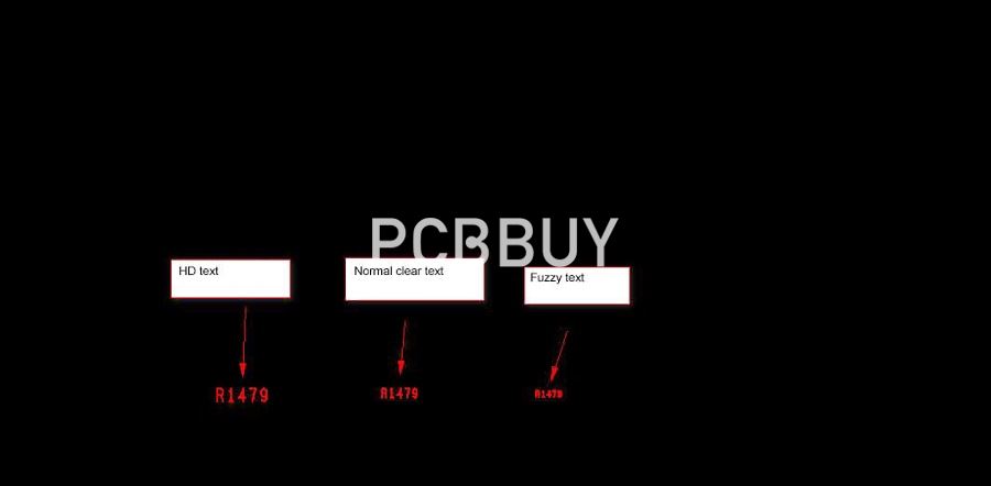
For text designs with line width less than 6mil or character height less than 36mil, we do not accept HD text requirements. For text designs with line width less than 5mil or character height less than 30mil, we do not accept text requirements that can be fully recognizable (there may be some fat blur). If the line width is less than 4mil or the character height is less than 28mil, please accept the blurring of text.
As for the design of such words mostly on the pad, our company will assume that your company has the assembly drawing available, and directly remove the words with the solder pad in the data, then the words will be unrecognizable on the finished product board, our company will not accept the complaint of such words being removed.
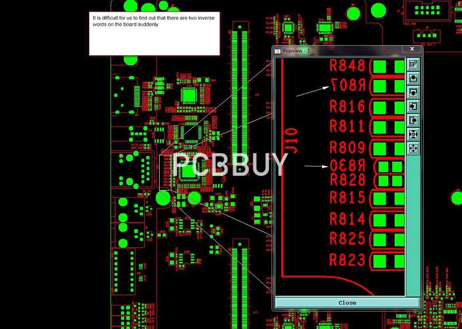
If your company has inverted characters in the engineering design, it will be difficult to find out when we are producing the engineering. We will try our best to find out, but we cannot accept such complaints of inverted characters.
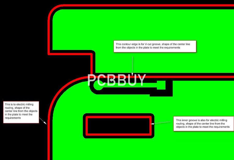
The electric milling position (frame edge and inner milling groove) needs to be 0.25mm away from the object in the plate, the V-cut needs to be 0.3-0.5mm away from the object in the boards, the thickness of the plate is 0.8mm and 0.3mm below, the thickness of the board is 0.8-1.0mm of 0.35mm, the thickness of the board is 1.0-1.6mm (including 1.6mm) of 0.4mm, The thickness of theboard is 1.6-2.0mm and 0.5mm. If the design data does not meet the above parameters, our company shall cut out copper according to the above parameters, and the finished products shall not expose copper (if your company has special requirements, the copper and articles in the board shall not be cut out, please note).
For boards with process edges panelized by us, our company will add 4 NPTH positioning holes of 2.0mm and 4 MARK optical matching points of 1.0mm on the process edge by ourselves. If the process edge is small, we will change the positioning hole to 1.5mm. If it is delivered by single board, we will not add any light spots and positioning holes.
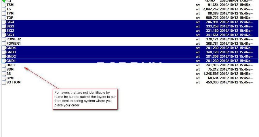
In order to improve efficiency and avoid unnecessary EQ questions, please provide the sequence of layers for multi-layer board s. We will give priority to the requirements of previous orders. If there are no requirements, we will refer to the name of Gerber on the data.
Layers unless your company specifically specified in the front desk to confirm, otherwise we are in accordance with our general rules. If the impedance board is within 2mil in line width adjustment, we will directly do impedance control and put into production of laminated structure, without tedious confirmation with your company (unless your company has special requirements).
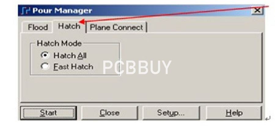
The pad copper mode of PADS can only be Hatch mode.
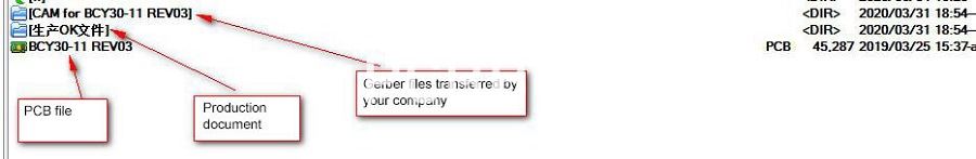
If there are both PCB files and Gerber files in the incoming files, we will take the Gerber file as the standard. If there are any production files, we will take the production file as the standard. (If the production document has no remark that it is a production document, we may make the board as the original design document). The above priority is: production file →GERBER file →PCB package file.
Our company only supports PCB files designed by Protel series software, AD series software and PADS software, and there are various versions of AD software. If it is designed by AD, please send Gerber files directly from your company, and we will make them according to the data transferred by your company. Because our company has hundreds of external engineers, and their software cannot be unified, our company will not accept complaints of functional errors caused by software version problems, nor will we bear any costs.
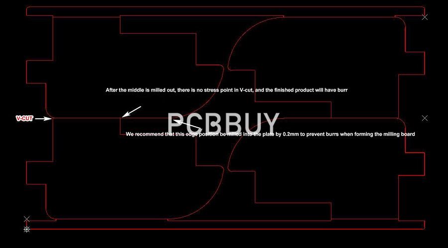
The edge indicated by the arrow is to make the V-cut process edge, but because the middle of the board has been electrically milled out, the V-cut knife has no force point when passing through, and the finished product will produce a slight burr on the edge of the board. This is a normal phenomenon, which will not affect the normal use of the board.
Documents in the package and writing requirements in Gerber are deemed invalid. Process requirements should be fully described in the process remarks when placing the order. Other remarks are invalid.
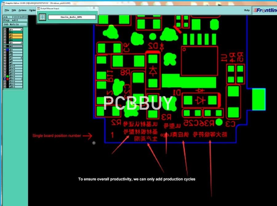
In order to increase the efficiency of board making and avoid unnecessary EQ questions, we will make such requirements as shown in the picture according to the data, and only one production cycle will be added.
When designing the panelization, if it is a super small board, we will jigsaw it. Only when the width of the direction of the non-V-cut is greater than 100MM, can we make the V-cut accurate. If the width of the direction of the two-direction V-cut is needed, we need to panelize the size of the jigsaw board greater than 100*100MM.
For this kind of design, there is no connection line in the same network, or the same network is only connected with a trace (connection bit less than 4MIL). We cannot guarantee that the circuit will be broken during the production process. Please connect the wiring of the same network completely in the design data, so that both sides will have a quality guarantee.
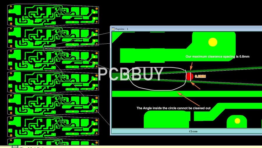
Similar to this type of board, there will be a very small and long acute Angle between the two boards after the panelization. Where the width of the acute Angle opening is less than 0.8mm, we cannot clear away the cloak at that distance, and we can only deal with it according to the data. Please pay attention to this situation when designing panelization.
We will redefine layers and attributes for all PADS designed documents. If the settings are not reset, turning out of Gerber directly will result in data redundancy or data messing. In order to Be consistent, we will redefine layers and attributes according to internal technical requirements. If there is any conflict or difference between the original Settings, our company will not be responsible. Finally, we suggest using PADS files. The most reliable method is to provide Gerber files from your company to ensure the accuracy of document execution.
For single-sided and double-sided documents, when the board thickness that your company orders is X, our production core board will be X-0.1mm. If your company's document is copper-free (bare board), there is a risk that the thickness of the finished plate will be too thin, because we need to select a production core plate according to the same thickness of the lower veneer. After order combination, the order of this bare plate will also be put into other boards of the same thickness. The other boards are copper-clad (the thickness is up to the standard), and the boards are copper-free (the thickness may be too thin).
For the opening and slotting of the outer layer, we only identify it in GKO (forbidden wiring layer). If we need to make the outer layer in the design, please make a separate comment.


