Phone:+86 18806715434
Service Time:China:9:00 - 18:00
China Time Zone(GMT+8)(Update in 5 mins)
Phone:+86 18806715434
Service Time:China:9:00 - 18:00
China Time Zone(GMT+8)(Update in 5 mins)
Our Service
PCBBUY specializes in 1-22 layer PCB prototyping and medium to large-scale production.
We focused on solving slow delivery and procurement difficulties for complex, high-difficulty, special, and multilayer-count orders.
8 Layers Board
10 Layers Board
12 Layers Board
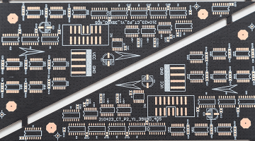
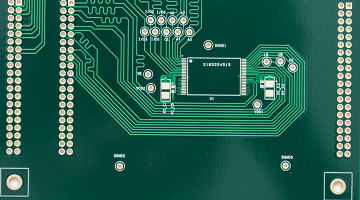
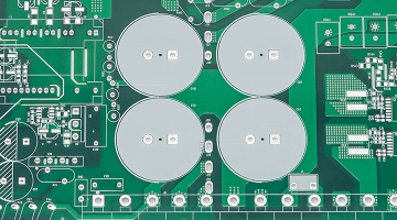
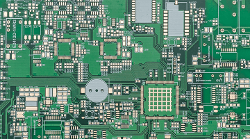
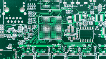
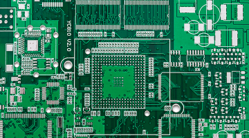
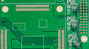
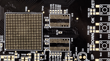
Product Display
High quality & short lead time customized service for global customer over 100000+ choose us
4 Layers Board
Material: FR-4
Application: P2 sidplay screen
Layer/board thickness: 4/1.6mm
Surface finish: OSP
Trace width/spacing: 3.00/3.00mil
Mininum hole size: 0.2mm
Technolugy: Tending via, high-precision
4 Layers Board
Material: FR-4
Application: Module boards set
Layer/board thickness: 4/2.0mm
Surface finish: ENIG
Trace width/spacing: 8.00/8.00mil
Mininum hole size: 0.4mm
Technolugy: Multistage impedance control
of inner & outer layer
6 Layers Board
Material: FR-4
Application: industrial control
Layer/board thickness: 6/2.0mm
Surface finish: HASL
Trace width/spacing: 3.00/3.00mil
Mininum hole size: 0.25mm
Technolugy: vias not covered/copper thickness
6 Layers Board
Material: FR-4
Application: industrial electronics
Layer/board thickness: 6/1.6mm
Surface finish: ENIG
Trace width/spacing: 3.00/3.00mil
Mininum hole size: 0.3mm
Technolugy: high-precision/ENIG
8 Layers Board
Material: FR-4
Application: CE
Layer/board thickness: 8/1.6mm
Surface finish: HASL
Trace width/spacing: 4.00/4mil
Mininum hole size: 0.2mm
Technolugy: vias not covered/copper thickness
8 Layers Board
Material: FR-4
Application: intelligent printer
Layer/board thickness: 8/2.0mm
Surface finish: HASL
Trace width/spacing: 3.00/3.00mil
Mininum hole size: 0.2mm
Technology: multistage impedance matching, \
high precision
10 Layers Board
Material: FR-4
Application: industry control
Layer/board thickness: 10/2.0mm
Surface finish: ENEPIG
Trace width/spacing: 3.00/3mil
Mininum hole size: 0.2mm
Technolugy: ENEPIG
12 Layers Board
Material: FR-4
Application: power system
Layer/board thickness: 12/2.0mm
Surface finish: ENIG
Trace width/spacing: 3.00/3.00mil
Mininum hole size: 0.2mm
Technology: high TG, thick copper
PCB maximum size 625×500mm
Minimum trace width/space of inner and outer layer 3mil
Technology: Buried Vias hole, edge plating, two-tone ink, PTH, counterbore
Impedance matching of inner & outer layerranges: 45-110Ω
PCB boards thickness 0.25-3.0mm
Minimum hole size 0.2mm , aspect ratio of board thickness and hole size 20:1
Solder mask: tenting vias/vias not covered/plugged vias/ Epoxy filled vias
Support single/double PP specific stackup
Quality Certification


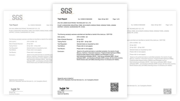
SGS is the world's leading testing,
inspection and certification company.
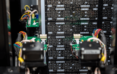
Core Technology
We have world-class PCB production equipment and high-precision testing equipment,
insist to produce high-quality products in essence
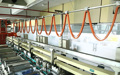
PTH & Plating
PTH & Plating
Gantry type vertical immersion line
Deep hole capacity reaches 13:1
Uniformity of copper plating more than 97% Pattern plating 70min
Hole wall copper thickness 18-22μm
Surface copper thickness ≥35um
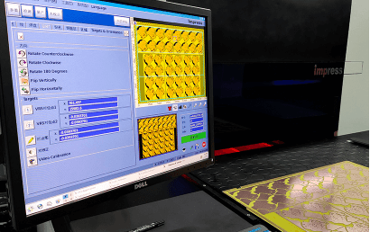
Circuit
Circuit
LDI layer exposure,circuit exposure is more accurate
DSE integration production
Effective control line too thin, micro-short, incomplete etching
Minimum trace width & spacing 2mil
AOI to avoid hidden quality issues
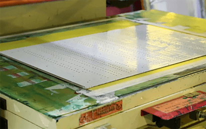
Solder Mask
Solder Mask
Automatic solder mask
80 min baking in a multi-temperature zone
Make sure the uniformity and adhesion of solder mask
Solve yellowing and exposed copper of annular ring
Solder mask ink meets international safety standards
Test
Test
High-speed flying probe testers
Maximum test speed 3000 points/min
Positioning resolution
HD CCD probe positioning accurately
Avoid open circuits, short circuits
Products & Service
Certification


Communication
Link us


