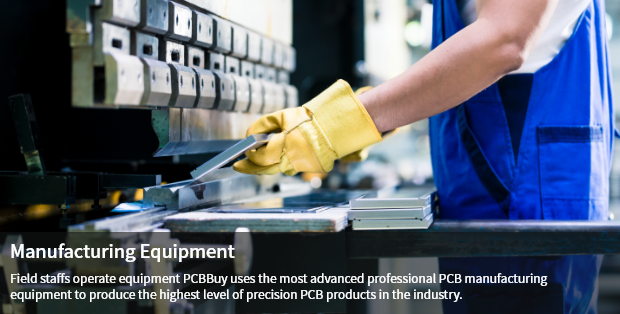
Vist our Profeceial Process of Manufacturing
PCB manufacturing is a complex process of many steps Each PCB has a unique function for a particular product. Check for main steps of multilayer PCB manufacturing. At PCBBUY, we promise to guarantee the quality of our boards through a product specification and quality control. In the production flow below you can see where the PCBBUY process is unique up to the IPC standard.
Single and double sided PCB
 Cutting
Drilling
Immersion
Plating
Pattern transfer
Etching
Cutting
Drilling
Immersion
Plating
Pattern transfer
Etching
 Solder mask
Silkcreeen
Surface finish
HASL/ ENIG
Prototyping
Solder mask
Silkcreeen
Surface finish
HASL/ ENIG
Prototyping
Inspection of
finish board
 OSP
Package
Put in storage
Shipment
OSP
Package
Put in storage
Shipment
Process of multilayer PCB
Inner Drilling
(immersion)
PTH
(back lighting)
Inner Plating
(QPLAIPQC)
Inner circuit
(AOI)
Epoxy filled vias
(AOI)
Stackup
Laser drilling
(CO2)
Outer drilling
(immersion)
PTH
(back lighting)
Electroplate
(QPLAIPQC)
Online AOI
Outer circuit
Solder mask
Silkcreeen
Surface finish
(ENIG/HASL/ENEPIG)
Finished PCB test
(flying probe)
CNC
(routing/V-CUT/Beveling)
Conductivity test
(special/automatic)
Low resistance test
Finished PCB test
Surface finish
(OSP/PTH)
Shipment test
(FQA)
Package
Shipment