3D AOI vs AXI Inspection in SMT Assembly
By:PCBBUY 10/26/2026 16:50
Introduction
As electronic assemblies become more compact and complex, reliable solder-joint inspection is essential for preventing manufacturing defects and improving product quality. Two commonly discussed technologies are 3D Automated Optical Inspection (3D AOI) and Automated X-ray Inspection (AXI).
Understanding 3D AOI vs AXI inspection in SMT assembly helps engineers select the right inspection strategy for different component packages, solder-joint structures, and reliability requirements. Rather than choosing one technology for every application, manufacturers should match inspection methods to the defects that need to be detected.
For automotive electronics, industrial control, power systems, energy storage, new-energy equipment, and embodied robotics, combining appropriate inspection methods with process control can improve assembly consistency and reduce the risk of defects reaching customers.
1. What Is 3D AOI Inspection?
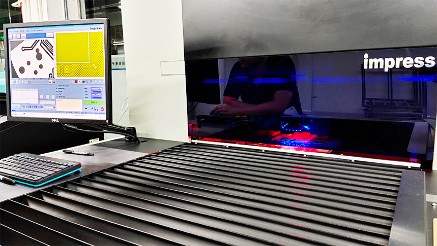
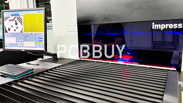
3D AOI uses optical imaging and three-dimensional measurement to inspect accessible features on an assembled PCB. Depending on the equipment and inspection program, it can evaluate component position, orientation, height, coplanarity, and visible solder-joint characteristics.
Typical applications include detecting missing or misplaced components, reversed polarity, skewed parts, lifted leads, visible solder bridges, and certain solder-volume or height-related abnormalities. Compared with conventional 2D AOI, 3D measurement provides additional geometric information that can improve defect recognition for suitable components.
However, optical inspection depends on visibility. Solder joints hidden beneath BGA or other bottom-terminated packages generally cannot be fully evaluated by ordinary optical imaging.
2. What Is AXI Inspection?
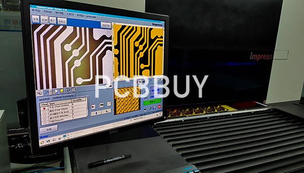
AXI uses X-ray imaging to inspect internal or concealed structures within an electronic assembly. Because X-rays can pass through component packages and reveal differences in material density, AXI is particularly useful for examining solder joints that are inaccessible to optical cameras.
Typical applications include BGA solder-joint inspection, hidden solder bridges, suspected open connections, and voiding patterns in applicable solder joints. The exact defects that can be detected depend on package geometry, image quality, inspection algorithms, and the acceptance criteria.
X-ray images also require engineering interpretation. For example, a measured void percentage should be assessed against the applicable component requirements and customer specifications rather than treated as automatically acceptable or defective.
3. 3D AOI vs AXI: Main Differences
|
Comparison factor |
3D AOI |
AXI |
|
Inspection principle |
Optical imaging with 3D geometric measurement |
X-ray imaging of internal structures |
|
Best suited for |
Visible component and solder-joint features |
Hidden solder joints and concealed structures |
|
Common applications |
Component presence, polarity, alignment, lifted leads, visible solder defects |
BGA joints, hidden bridges, suspected opens, solder-joint voiding |
|
Main limitation |
Cannot reliably inspect solder joints fully hidden beneath packages |
Image interpretation can be affected by overlapping structures and package geometry |
|
Typical role |
Broad inspection of accessible assembly features |
Targeted or inline inspection of concealed joints |
|
Relationship to the other method |
Does not replace AXI for hidden-joint inspection |
Does not replace AOI for all visible placement and surface defects |
The best choice depends on the assembly's component mix and quality risks. For many SMT products, 3D AOI and AXI are complementary rather than competing technologies.
4. How to Choose the Right Inspection Strategy
A practical inspection plan begins with the PCB assembly design and its potential failure modes.
-
Use 3D AOI for visible assembly features. It is useful for checking component placement, orientation, lead condition, and visible soldering characteristics.
-
Use AXI for critical hidden joints. BGA, QFN, and other bottom-terminated packages may require X-ray inspection when their solder joints cannot be adequately assessed optically.
-
Combine inspection with process controls. Solder Paste Inspection (SPI) evaluates solder paste deposits before reflow, while ICT or functional testing can verify electrical connectivity or product behavior within the test's coverage.
-
Define acceptance criteria before production. Inspection thresholds should reflect the component manufacturer's recommendations, applicable IPC requirements, customer specifications, and the intended operating environment.
For automotive, industrial control, electrical power, power supply, energy storage, new-energy, and embodied robotics applications served by PCBBUY, inspection coverage should reflect the consequences of potential failure. High-reliability applications may require additional verification, but inspection scope should be agreed upon rather than assumed from the industry label alone.
5. PCBBUY SMT Assembly and Quality Control
PCBBUY's published SMT assembly information describes an inspection workflow that includes SPI, AOI, X-ray inspection for packages such as BGA and QFN, and electrical or functional testing where required. These methods support different stages of quality control, from solder paste printing through final assembly verification.
A typical process may include incoming PCB inspection, solder paste printing, SPI, component placement, reflow soldering, AOI, X-ray inspection for selected hidden-joint packages, and the agreed electrical or functional tests.
For shipment acceptance, the inspection plan should be aligned with the purchase order, applicable IPC-A-610 class where specified, and customer requirements. Final inspection and test records should reflect the actual scope performed. The availability of a particular 3D AOI configuration or a specific X-ray inspection method should be confirmed with PCBBUY during quotation and engineering review.
By coordinating inspection requirements early, customers can avoid gaps between the quality evidence they expect and the tests included in the production plan.
Conclusion
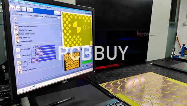
The difference between 3D AOI and AXI comes down to what each method can see. 3D AOI provides optical and height-related information about accessible assembly features, while AXI reveals concealed solder-joint structures that cameras cannot directly inspect.
For reliable SMT assembly, the inspection strategy should be based on package type, defect risk, product reliability requirements, and agreed acceptance criteria. PCBBUY supports SMT assembly quality control through its published AOI, X-ray, SPI, and electrical or functional testing workflow, with project-specific inspection requirements confirmed before production.
FAQ
1. What is the main difference between 3D AOI and AXI?
3D AOI uses optical imaging and three-dimensional measurement to inspect visible assembly features. AXI uses X-rays to inspect concealed structures, especially solder joints beneath components.
2. Can 3D AOI detect BGA solder-joint defects?
It can inspect accessible features around a BGA package, but it generally cannot directly verify solder joints hidden underneath the package. AXI is commonly used for that purpose.
3. Does AXI replace 3D AOI in SMT assembly?
No. AXI is suited to hidden structures, while 3D AOI is useful for visible placement and soldering features. Using both may provide more complete inspection coverage when the design and risk assessment justify it.
4. Is AXI required for every SMT assembly?
No. The need for AXI depends on component packages, product reliability requirements, customer specifications, and the risks associated with hidden solder joints. Some assemblies may need targeted X-ray inspection rather than inspection of every board or component.
5. What inspection services should I confirm with PCBBUY before production?
Confirm whether AOI, X-ray inspection, SPI, ICT, functional testing, and any required inspection reports are included in the project. Specify critical component packages, applicable IPC-A-610 class, customer acceptance criteria, and any special reliability requirements before production starts.
Industry Category