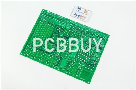
4 layer pcb design rules
By: 01/11/2024 18:38

With the rapid development of electronic technology, the application of multilayer printed circuit boards (PCBs) is becoming increasingly widespread. As one common type of multilayer board, four-layer PCBs possess high integration and stability, making them widely utilized in various fields. This article will provide a detailed introduction to the design rules of four-layer PCBs to ensure their performance and reliability.
Layer Stackup
The layer stackup of a four-layer PCB typically consists of signal layers, ground layers, power layers, and insulation layers. The signal layer is primarily used for routing circuit signal lines, the ground layer provides a path for signal return and reduces electromagnetic interference, the power layer offers power distribution, and the insulation layer ensures insulation between layers. During design, careful consideration should be given to the functions and relationships between layers, with a rational arrangement of layer order and thickness to ensure overall stability.

Routing Design
In the design of four-layer PCBs, routing design is one of the most crucial aspects. Parameters such as trace width, spacing, and layout patterns will impact signal quality and transmission rates. Depending on the characteristics and requirements of the signals, appropriate trace widths and spacings should be selected. Additionally, employing right-angle or rounded corner transitions can help reduce signal reflection and crosstalk. Furthermore, efforts should be made to minimize trace lengths and curvature to enhance signal transmission efficiency and stability.
Impedance Control
Impedance is an essential parameter for assessing the performance of PCB traces. In the design of four-layer PCBs, impedance values for traces should be calculated and controlled based on actual needs and signal standards. Common methods for impedance control include adjusting trace width, changing copper thickness, and using impedance control materials. Through effective impedance control, signal loss and distortion during transmission can be minimized, enhancing signal quality and stability.
Power and Ground Design
Power and ground design is a critical aspect of four-layer PCB design. To minimize noise and interference between power and ground, multi-layer grounding techniques should be employed. Ground layers can be segmented into different areas based on signal characteristics and requirements. Simultaneously, careful consideration should be given to power distribution and decoupling, with the rational placement of power planes and decoupling capacitors to ensure power stability and reliability.
Reliability Design
Reliability design is indispensable in the design of four-layer PCBs to ensure long-term stability and reliability. Measures such as reinforcing component fixation and heat dissipation design, strategically placing vias and pads, and enhancing insulation layer protection should be implemented. Additionally, environmental adaptability tests and lifespan assessments should be conducted to guarantee the reliability and stability of the PCB in practical use.
Maintainability Design
Maintainability design involves considering requirements related to the repair and replacement of the PCB during the design process. Proper arrangement of component layout and interface positions facilitates ease of maintenance and replacement. Selecting suitable connectors and interface standards can improve compatibility and expandability. Maintainability design contributes to prolonging the lifespan of the PCB, reducing maintenance costs, and enhancing overall reliability.
Conclusion
This article provided a detailed introduction to the design rules of four-layer PCBs, covering layer stackup, routing design, impedance control, power and ground design, reliability design, and maintainability design. In practical applications, a comprehensive consideration of various factors and the development trends of new technologies and materials is essential to formulate suitable design schemes, ensuring the performance and reliability of four-layer PCBs. Continuous optimization and improvement of design rules and technological levels should be pursued in response to evolving technologies and materials.
If you want to order PCB product, please check and custom your order online.
Industry Category


