PCB Layout Guidelines: 5 Aspects of Power Integrity Analysis in PCB
By:PCBBUY 09/24/2021 09:28

The circuitry on a modern PCB needs its voltage and current to be maintained at its required levels within its power delivery network (PDN) with very little change. Problems like these can cause you a lot of effort in the debugging stage, as you trying to find and correct them. To avoid these headaches, it is important to create a printed circuit board design with a good PDN in it.
In this passage, we will help you to get into know the professional knowledge. If you are curious about Power Integrity Analysis in PCB, please check and read the content for more information.

What are the 5 aspects of power integrity analysis in PCB?
1. What are the common issues of power integrity in PCB?
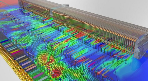
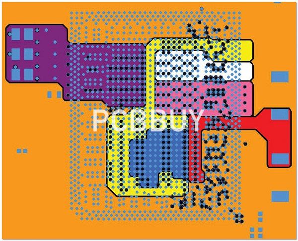
Every circuit board will have some common power integrity problems that need to be identified by examining the PDN. The PDN impedance, S-parameters, Z-parameters, DC current density, and voltages are all important points to examine and calculate as part of power integrity analysis of an electronic system. In some systems, power integrity problems are minor and may not be noticed in measurements. However, in high-speed PCBs with fast signal edge rates, many common power integrity issues can be observed and can lead to system failure.
Some of the common power integrity problems that can occur in a circuit board include:
· High PDN AC impedance and/or DC resistance
· Power rail collapse and ground bounce
· Radiated emissions due to weak decoupling
· Excessive heat generation
· ESD at high voltage
2. What are the challenges for nice power integrity in PCB?
Back when the devices on a board were simpler in nature, and only had one power and one ground connection, the noise tolerances were not as tight. You could easily control excessive noise with an extra capacitor. The switching speeds in those devices also didn’t create the same problems as the high speed devices of today do.
With the processor chips today on large ball-grid array (BGA) packages, the power requirements are much more intense. There is hundreds of power and ground pins in these devices, and each device may require multiple supply voltages with some of those voltages going down to less than one volt. These pins are also pulling many amps of current for the processor to do its job, and to provide “clean” power requires a huge network of capacitors.

3. How to achieve best power integrity in PCB?
Managing power integrity on your PCB can be viewed as designing your board such that power supply output variation is minimized, interference between traces and the PDN is minimized and power losses and dissipation are adequately managed. These objectives can be simultaneously achieved by employing the following tips into your design process.
· Make good use of capacitance and filters
· Utilize trace parameters to control route impedances
· Use separate grounds for digital and analog signals
· Use regulators on power supply inputs
· Select materials to help control impedance
4. What are the power integrity fundamentals?
Ground Bounce
With the increased switching rates in high-speed designs, the low state of a signal may not return all the way back to the reference ground level. This ground bounce is also known as simultaneous switching noise or SSN.
Power Ripples
The switching of an SMPS (switched-mode power supply) can cause power ripples to spread out through the design. These ripples could potentially create crosstalk, overwhelming and disrupting the operation of nearby circuits.
Electromagnetic Interference
The switching of an SMPS between its on and off states can create EMI if not designed correctly. Not only will EMI affect the smooth operation of the circuitry on the board, but it can also interfere with external electronics.
Signal Return Paths
Although clear signal return paths are part of creating good signal integrity, reference planes are part of the board’s PDN system and must be considered when designing for power integrity. High-density parts will have a number of vias for signals and connections to power and ground, but these vias can block the clear return paths on the reference plane.

5. What are the useful tips of power integrity in PCB?
When laying out a PCB design, here are some areas to pay close attention to in order to avoid some of the power integrity issues that we’ve been discussing.
Board Layer Stackup Configuration
The PDN of a board is closely tied to the configuration of the layers in the board stackup.
Component Placement
Reference voltages must be carefully managed in your PDN to ensure that the components receive the power they need.
Trace Routing
When routing from power pins to bypass capacitors, keep the traces as short as possible.
Planes
It is always best to use a solid plane for grounding instead of routing ground with traces.
Industry Category


