5 Challenges of Etching PCB Boards at Home
By:PCBBUY 09/16/2021 09:14

There are many advantages of etching your own circuit boards at home. You could get prototype PCB quickly after etching and it’s also convenient. Copper is removed from the board except at the places where wired connections are present. The advantages include de-cluttering of the system and ease of seeing the connections and an increase in usability and portability.
In this passage, we will tell you everything about the DIY PCB etching. You can find all the knowledge of etching PCB at home. If you are curious about this topic, please check and read the passage we prepare for more information.
If you want to order PCB product, please check and custom your order online.
Why is etching PCB at home difficult?
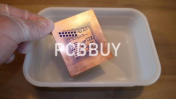
To hand make a PCB, an engineer must first build the PCB and etch out the copper traces. Best practices dictate copper traces be etched by submerging the PCB into a fluid compound of ferric chloride to dissolve the top layer of photoresist and reveal the traces beneath. Moreover, these traces must be equally exposed across every PCB build to prevent stray variables from sparking an error or malfunction. In addition, as etchant becomes saturates with copper it becomes increasingly ineffective, which makes consistent etching by hand even more difficult.
What are the considerations for etching PCB at home?
You can etch a PCB by yourself, in a lab or even at home, through a simple and inexpensive production process. It makes sense when you wish to produce a single or a very small number of boards and want to avoid manufacturing costs. The etching process is therefore effective for a small workshop. There are however some issues to consider:
1. There is a risk of injuries due to the chemicals involved.
2. The quality of the results depends on several factors which you won't be able to master completely the first time. This can be somewhat compensated by using good machinery.
3. There is the problem of waste disposal. Toxic chemicals require a proper disposal service.
To learn how to etch a PCB, make sure that your Fritzing PCB design is complete and exported as an etchable PDF or SVG, then follow these instructions.
What are the 5 challenges during the etching PCB at home?
1. The PCB application could not be determined
Etching printed circuit boards are highly related to the function or the role of the PCB. Engraving gets rid of excess copper to reveal the predetermined desired circuit pattern. There are several PCB etching processes that designers use. You choose all of these depending on the function of the PCB.
Unfortunately, though, plenty of PCB enthusiasts don’t understand that etching a PCB is related to the purpose of the PCB. To ensure the quality of your PCB, DIY at home is difficult to guarantee.
2. We don’t have professional equipment to process
During the PCB etching process, it is necessary to prepare kinds of professional equipment. Unfortunately, a majority of DIY PCB enthusiasts lack the professional equipment necessary for carrying out PCB etching on their own. For example, if you don’t have rubber gloves, your hand may end up getting strained. Therefore, having the right equipment is essential to etch a PCB that will function as desired.
3. It’s difficult to control the etching time
During the etching process, there is a need for several chemicals when creating the proposed layout. Copper etching a PCB requires reagents such as Ferric Chloride and Ammonium. Besides, if you want to ensure that the etching process runs smoothly, you must control the etching reagent at specific temperatures in certain time.
4. The process is too complex to control
It is a highly complicated process that, when done wrong, may lead to the production of ineffective printed circuit boards. Since etching PCB is not an easy process, as you may imagine. Do you have the necessary tools and chemical reagents essential for etching your printed circuit boards? How do you specify the thickness of your PCB when making it by yourself? You may need to seek a professional's services for assistance.
5. The PCB coating will be destroyed
Professional PCB makers understand how to develop glossy PCB surfaces that come with plenty of benefits. The most significant difference between a gloss finish on a PCB and a matte finish is more aesthetically. By hiring a professional, you’ll be in a better position of being provided with a PCB containing a high-quality gloss finish. However, by etching PCB at home, you’ll lose the gloss of your PCB's coatings.
Conclusion
As explained above, apparently making PCB at home looks pretty simple, and it is just a matter of a few hours to create outstanding professional grade PCBs using ready to made DIY materials from the market. That said, the process may require some caution and precision for achieving the desired results, so that the intended circuit project is accomplished successfully.
Industry Category


