5 Common PCB Design Mistakes
By:PCBBUY 07/02/2021 17:30

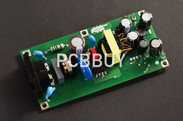
As a very essential step of the PCB manufacturing process, PCB design will influence the quality and performance of the finished boards. PCB designers need to avoid fabrication errors while designing printed circuit boards. Production costs often increase due to PCB design errors .As a result, PCB designers need to avoid fabrication errors while designing printed circuit boards.
In this passage we will lead you to learn the common mistakes of PCB design. Please follow us and check for more information from the content below.

1. Incompetent layout techniques
PCB designers must be able to develop excellent layout designs for the proper functionality of components that use printed circuit boards. Lately, there is a huge demand for PCBs with minimal footprints. Printed circuit board designers are therefore required to employ the use of smaller components that reduce footprint significantly. Generally, components that find use here are very close to each other.
If you happen to select an incompetent layout technique, then the connection may go wrong and affect the functionality of where it will find useful. Sadly, most printed circuit board manufacturers find it hard coming up with the best layout. The greatest challenge faced is when handling the device with higher pin counts and a smaller pitch. If the layout is wrong or incompetent, rest assured that the board will fail to function as desired.
To ensure the desired functionality, it is very important to select the best layout technique available in the market. If you are in the market for the best PCB designer, look no further after comparing several companies. They must understand nearly everything to do with the board layout and ready to assist you all the way. Whether they are simple or complex layout designs, they must have the right personnel with the best techniques to assist you. They must understand how poor PCB layout affects the productivity and credibility of a PCB designer. Choose a reliable company for the best PCB layouts.
2. Wrong/Incorrect designing tools
If anything, having the right tools or equipment in place is a fundamental step needed for a successful printed circuit board design. With the right tools, rest assured of a board that functions well in the intended place. Choosing the wrong equipment will bring about problems such as increased costs of manufacture and delayed time in creating the board's design. If you look around, there are high chances that there are plenty of printed circuit boards in the market designed using incorrect designing tools.
Again, a majority of printed circuit board manufacturers seem to struggle with this problem a lot. Many of them find it a bit challenging in their choice of tools to use. It is always recommended to use the right tools that suit all your design needs. Opting for substandard printed circuit board design tools will lead to a board that won’t meet its intended needs. However, all is not lost since there are several easy-to-use tools such as electronic design automation software packages.

A professional company always ensures that they employ several design tools to come up with a board whose functionality is unquestionable. The designers employ many of these tools, depending on where the circuit board will find its use. Again, if you happen to be in the market for a manufacturer with a huge list of PCB design tools, look no further after comparing. It is very important to carry out a proper analysis and homework and choose the right equipment that suits all your needs.
3. Landing pattern errors
Landing pattern errors are equally another huge challenge that most printed circuit board designers currently in the market find it challenging. Landing pattern errors are lately coming in as another challenge during the boards’ design face affecting many designers out there. Printed circuit board landing patterns are made up of a huge library of electric mechanisms known to use schematic symbols.
Conclusion: there is little or no challenge to printed circuit board designers who follow the design through and thoroughly. However, if the libraries are not followed as desired, then drawing the schematic symbol by hand is another way. But important to note here is that it is very easy to make mistakes when drawing the landing pattern manually. Such mistakes may also end up increasing the chances of errors.
A professional company will not find or constantly report issues to do with landing pattern errors that much with pride, though. They will employ several electronic components and software packages in our printed circuit boards to ensure functionality. It is very easy to make costly errors when drawing your landing pattern. For example, if you get the pin-pin spacing wrong even by a millimeter, it will be a bit hard or tasking to solder on the circuit board.
4. Decoupling incorrectly located capacitors
Critical components of the board require a clean and very stable source of voltage. But for decoupling capacitors to function as desired, they must be close to the pin that requires the stable voltage. Sadly, most PCB designers struggle with this, leading to components that don't work in the right way.
It is also critical to ensure the placing of the output capacitor meant for power supply as close as possible to the regulators' output pin. By doing so, the optimization of stability gets optimized in addition to an improvement in transient response. Still, rest assured that your board will fail in terms of functionality if you get it wrong.
Printed circuit board designers have to ensure that they utilize the decoupling capacitors in the right way. Professional companies have industry-tested experts with the ability to decouple capacitors with a lot of ease. If the placement of capacitors is incorrect, they will not work properly and affect the device where it will be in use.
5. Failure to backup the work
To achieve the perfect results during the design process, you can do so using some software and data. A good example is the electronic design automation software that assists many designers in coming up with complex printed circuit board designs. Based on the software's high speeds and flexibility, it is very easy to lose the data even before saving them.
To ensure that such important data is not lost, it is essential to ensure that you save your data as often as possible. If necessary, printed circuit board designers need to ensure that they come up with save points. By creating such savepoints, even if a single storage point gets spoilt, the others will remain saved and secured. With a backup in place, there are no reasons to worry if one or two complex designs are lost.
Professional companies understand the importance of backing up the printed circuit board designs regardless of whether they are simple or complex. The entire designs are safely backed up, and no chance of the data getting lost.
Industry Category


