5 Effective Methods PCB Quality Control and Testing Methods
By:PCBBUY 11/11/2021 09:25

Printed Circuit Boards are the most used and basic assembly unit applied by all types of electronic devices. All functions and performance of devices are implemented mainly by PCBs. PCB is the heart of electronic devices and both their quality and reliability is directly correlated with quality and reliability of electronic equipment. Nowadays, intelligence and miniature of electronic devices leads to increasingly smaller size and complicated structures of PCBs.
If you are going to learn more about methods to control the quality of PCB, you can choose us. Please check and read the content below we prepare for more professional information. You could get everything about control the quality of PCB.
1. How to check and confirm the quality of PCB?
PCB designers have to check and confirm the design drawings that will be applied by manufacturer for many times prior to manufacturing. Since PCB design can't be successful just after one trial and modifications have to be made time and time again, PCB manufacturers will hold multiple versions of design drawings. So it's necessary to carefully check and confirm the final design drawing provided by manufacturer prior to practical manufacturing so that manufactured PCBs conform to requirement of the last version.
2. How to pay attention to the quality of PCB in design?
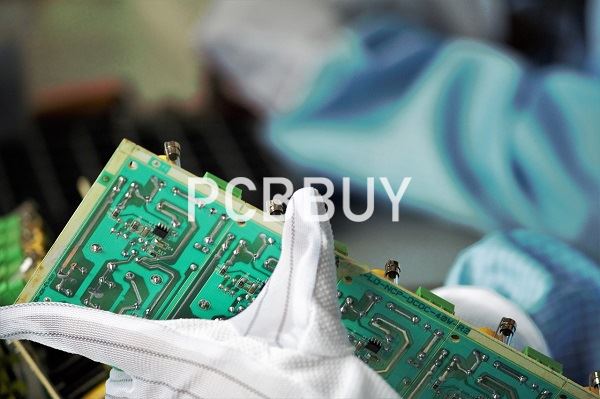
The quality of key procedures of PCB manufacturing influences a lot on performance and reliability of PCBs and quality control on that has to be strengthened. The key technological procedures formulated by PCB manufacturer have to be monitored and checked including etching, via mentalization etc. so as to ensure absence of burr, gap, bridge defect and void. Furthermore, quality control has to be overtaken on stacking of multi-layer PCBs in order to ensure the thickness, adhesive intensity and positional accuracy. Since gold plating is usually required by high-frequency PCBs and micro-strip boards, specific gold plating operation instructions have to be made in order to ensure the thickness and purity of plating plane.
3. How to process in-circuit testing?
In-circuit testing (ICT) is the most robust type of PCB testing in existence. The high price reflects that -- tens of thousands of dollars, though the cost will depend on board and fixture size, among other factors.
An ICT, also known as a bed-of-nails test, powers up and actuates the individual circuitry on the board. In most cases, the test is designed for 100% coverage, but you’ll get closer to 85-90% coverage. The nice thing about ICT is that the 85-90% you get is totally free of human error.
This test involves using fixed probes laid out in a way that matches the design of the PCB. The probes checks the integrity of the solder connection. The bed of nails tester simply pushes the board down on the bed of probes to start the test. There are access points predesigned in the board that allows the ICT testing probes to make connections with the circuit. They put a certain amount of pressure on the connection to make sure it stays intact.
ICT is often performed on bigger connections and ball grid arrays (BGAs). This test is for a “mature” product with very few revisions expected. If you don’t have design-for-manufacturing as part of your goal, with the proper pads on the board, you may not be able to use an in-circuit test. Unfortunately, you can’t change your mind and move to an ICT strategy halfway through production.

4. How to process AOI testing on PCB?
AOI uses either a single 2D camera or two 3D cameras to take photos of the PCB. The program then compares the photos of your board to a detailed schematic. If there is a board that does not match the schematic to a certain degree, the board is flagged for inspection by a technician.
AOI can be useful for detecting issues early to ensure production is shut down ASAP. However, it does not power up the board and may not have 100% coverage for all part types.
Never rely solely on an automated optical inspection. AOI should be used in conjunction with another test. Some of our favorite combos are:
· AOI and flying probe
· AOI and in-circuit test (ICT)
· AOI and functional testing
5. What are the benefits of controlling the quality of PCB?
Many companies see PCB testing as an absolute must due to the many advantages it provides them. Check out some of the following top advantages of PCB testing:
Increased safety
Since PCBs are often used in essential electronic technologies, their failure can cause major issues for a company’s productivity or an organization’s ability to perform essential services. A defective PCB could cause a fire, potentially putting those near it in danger.
Time savings
PCB testing in the early stages can help save time in the long run, allowing designers to identify major issues during the prototyping stage. Thorough testing enables designers to determine the root cause of each problem posed quickly and easily, making adjustments so that they can move on with production at a faster rate and reduce product lead-time.
Cost reduction
PCB testing prevents wasteful production of faulty products by using prototypes and small-scale assemblies to test the products. By completing thorough testing early in the design process, designers can prevent wasteful full-scale assemblies of faulty PCBs, ensuring that the design is as flawless as possible before it goes into production.
Industry Category


