5 Effective Tips of Design for Testability Guidelines in PCB Manufacturing
By:PCBBUY 03/29/2022 09:58

Designing for testability in a PCB design (DFT) is a critical step in the design for manufacturability (DFM) process. This critical concept boils down to developing a consistent product for the lowest possible manufacturing cost while maintaining an acceptable rate of defects. Considering testability throughout the PCB Design involves outlining the creation process to understand test point requirements and isolate faults quickly.
Do you know the design for testability guidelines in PCB manufacturing? If you are going to learn more professional knowledge about testability guidelines in PCB, please check and read the content below for more in this passage.
What are the considerations of testability guidelines in PCB manufacturing?
The first step that a contract manufacturer will take when reviewing a design for test is to consult the customer test specification that has been provided. With this information, a test method can be developed to cover the specifications. Although the CM test engineers can create their own specification if necessary, it is a good practice for you to give your CM as much information as possible so the board is fully tested to the customer’s expectations.
The CM will include marking up the schematic with test and connection points as part of their test review, as well as examining the layout. It is another good design practice to include specific test points in the schematic to help the CM with this preparation. The design review combined with the test methodology will help determine the type of fixture that is needed and if any modifications to the design are warranted to increase the effective fault coverage of the test procedures. All of this information is then incorporated into a test instruction (TI) document accompanied by descriptions, illustrations, and expectations for the test technicians to use during actual testing.
What are the main types of tests in PCB manufacturing?
Quality Assurance Testing
The electrical testing methods utilized by CMs can be classified by purpose. Tests conducted to measure your board’s connectivity fall under quality assurance or control. These quality checks may include:
· Impedance testing is performed to ensure there are no open circuits along traces or breaks between soldered connections.
· Continuity testing is done primarily to test the direction of current flow through components, such as diodes.
· Invasive tests, such as sawing, are employed to inspect the board’s internal structure (e.g. layers, vias).
· Most CMs utilize manual or automated inspections as part of their QA regimens. To have any of the above testing methods performed, a request may be necessary. However, none of the above tests require any dedicated design activity prior to manufacturing.
Design for Testability (DFT)
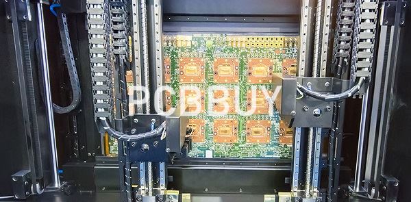
DFT, as the name implies, does require specific design actions to be performed before it can be applied during the manufacturing stage of product development. This generally means adding test points to the board such that parameters of interest can be calculated or measured for direct determination. There are basically two tests that fall under DFT: the flying probe test and the bed of nails test.
Flying Probe Test
The flying probe test is a non-invasive in-circuit test (ICT) to measure open/short circuits, values for passive components and continuity. This test is designed to be applied for prototypes and low production runs. Utilizing the flying probe test is a joint activity that requires the following steps by the PCB designer and CM:

What are test points and test structures?
Successful design for testing requires designating important test points in your PCB design files, which will then be used by your CM for a variety of tests. Test points are used to pinpoint specific circuit blocks and components you need to evaluate, as well as to designate the electrical functionality you expect from your design.
For high-speed/high-frequency designs, where signal integrity and power integrity problems are a primary concern, there are standard test structures you can place in your board. These test points and test structures will be used in subsequent bare-board and circuit tests to evaluate functionality and signal integrity.
Test points and test structures are normally designated in your schematic as no-BOM components. They can then be placed in your layout using your CAD tools. Most PCB CAD software will allow you to designate a via or a pad on a component as a test point. Alternatively, you can define a test point as a custom-designed pad in your layout. These are usually circular pads with 25 mil to 40 mil diameter. The same idea applies to test structures, although these structures have very specific geometries that are designed for evaluating specific aspects of signal integrity.
For advanced designs that require precise impedance control, it is infeasible to test interconnect impedance and signal attenuation in an assembled board unless you’ve designed your board for a boundary scan (JTAG). If you’re unsure of your designed interconnect impedance, you might consider producing a test coupon and requesting impedance measurements before finishing your layout and selecting test points or test structures. This is a low-cost pre-layout solution that helps you perfect your design before moving to manufacturing.
Industry Category


