5 Effective Tips of PCB Gold Finger Plating Process
By:PCBBUY 10/10/2021 10:37

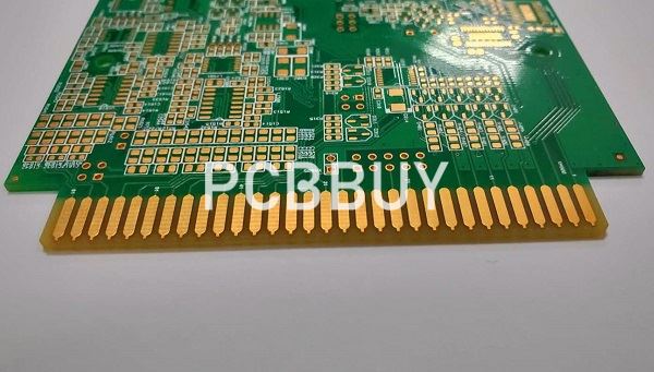
Gold fingers are the gold-plated columns that you see along the connecting edges of printed circuit boards (PCBs). The purpose of gold fingers is to connect a secondary PCB to the motherboard of a computer. PCB gold fingers are also used in various other devices that communicate via digital signals, such as smart phones and smart watches. Gold is used for the connecting points along a PCB because of the alloy’s superior conductivity.
In this passage, we will focus on the PCB gold fingers and the methods of processing PCB Gold fingers. If you are looking for more interesting information of PCB Gold fingers, please check and read the content for more knowledge.
What are the 5 tips of PCB gold finger plating process?
1. What are the main types of PCB gold finger plating?
There are two types of gold applicable to the PCB gold finger plating process:
· Electroless Nickel Immersion Gold: This gold is more cost-effective and easier to solder than electroplated gold, but its soft, thin (typically 2-5u” composition renders ENIG unsuitable for the abrasive effects of circuit board insertion and removal.
· Electroplated Hard gold: This gold is solid (hard) and thick (typically 30u”), thus more ideal for the abrasive effects of constant PCB usage.
Gold fingers make it possible for different circuit boards to communicate with one another. From the power source to the device or equipment, signals must pass between several contacts for a given command to be enacted.
2. What is PCB gold finger beveling?
Have you found out that the edges of PCB gold fingers are in slope forms? Well, the procedure of beveling allows sharp, square edges to turn into slopes. In the case of PCBs or printed circuit boards, the beveling process completes the surface finish. The beveling process of the gold fingers of a PCB gets initiated after completing the disposition of solder masks. The process of PCB gold finger beveling is unavoidable in terms of making insertions quicker and more effortless. Unless the gold finger beveling is completed, insertions will be more difficult than usual.
As you have already known about the beveling process, you also have to know which angle you are supposed to bevel the edges. Usually, PCB gold fingers are beveled at angles of 30 or 45 degrees to ease up the particular slot’s insertion process. Anyway, engineers and technicians bevel PCB gold fingers according to the requirements of the clients. The beveling angle of gold fingers also depends on the size of a particular circuit board.
3. What are the standards of PCB gold finger plating?
There are some standards you need to follow for the gold fingers so that it can work correctly during the plating process of gold finger. As well as the PCB design need to take into account the areas where is necessary to proper finger length and alignment. The rules can be used for the gold finger design as the follows no matter what the size or the purpose of the circuit board:

1. Plated through hole should far away from the gold fingers;
2. There should be kept at a distance between gold fingers and solder mask or screen printing;
3. Gold fingers should always keep the opposite direction from the middle of the board.
If you don’t follow these rules during the plating process of PCB gold finger, the circuit board may be unable to communicate with the parent board. Alternately, the board might not be unsuitable for the corresponding slot on the motherboard.
4. What are the specifications of PCB gold finger plating?
· Do not locate plated through holes near the gold fingers.
· The gold fingers should not have solder mask or screen printing near them.
· Always orient the gold fingers so they face opposite the center of the PCB.
5. What are the surface finished of PCB gold finger plating?
Electroplated nickel gold: Thickness up to 3-50u", due to its superior conductivity, oxidation resistance and wear resistance, it is widely used in gold finger PCB that require frequent plugging or PCB board that require frequent mechanical friction. While the cost of gold plating is extremely high, it is only applied to local gold plating such as gold fingers.

Immersion Gold: The thickness of conventional is 1u", up to 3u". It is widely used in high-precision PCB board with button position, bonded IC, BGA, etc. due to its superior conductivity, flatness and solderability. The gold finger PCB with low wear resistance requirements can also choose the entire board immersion gold process. The cost of the immersion gold process is much lower than that of the electric gold process. The color of the immersion gold process is golden yellow.
Industry Category


