5 Essential Aspects of PCB ICT Guidelines in PCB Manufacturing Process
By:PCBBUY 10/28/2021 09:34

There are three general areas for the board designer to be concerned about. First, it is necessary to determine what connections are needed from an electrical standpoint. Once this is determined, there are the mechanical concerns about how to provide areas for the probes to contact and how to align the board.
Are you going to learn more about PCB ICT? In this passage, we will provide everything about PCB ICT, please check and read the content for more information.

1. How to process location holes for PCB?
In order that the connections can be made to the board, it is necessary to have accurate position or location holes that can be used to accurately locate the PCB onto the test fixture. In this way the PCB board can make accurate location onto any probes or connections required. Requirements for the tooling holes may include:
· Three preferred but a minimum of two, on opposite diagonal corners
· Tooling or location holes should not be plated to ensure their accuracy
· Tooling or location holes should not be obscured and they should be free from components etc in the vicinity of the hole to enable any locating spigots on the test fixture to mate with the hole.
· Location accuracy of the tooling or location holes should typically be within 0.05 mm, i.e. 0.002 inches, although with techniques changing all the time, check the requirements for the actual tester..
2. What are the considerations before PCB ICT?
The first step that a contract manufacturer will take when reviewing a design for test is to consult the customer test specification that has been provided. With this information, a test method can be developed to cover the specifications. Although the CM test engineers can create their own specification if necessary, it is a good practice for you to give your CM as much information as possible so the board is fully tested to the customer’s expectations.
The CM will include marking up the schematic with test and connection points as part of their test review, as well as examining the layout. It is another good design practice to include specific test points in the schematic to help the CM with this preparation. The design review combined with the test methodology will help determine the type of fixture that is needed and if any modifications to the design are warranted to increase the effective fault coverage of the test procedures. All of this information is then incorporated into a test instruction (TI) document accompanied by descriptions, illustrations, and expectations for the test technicians to use during actual testing.

3. What is the basic equipment for PCB ICT?
Even when ICs fail, one of the major reasons is static damage, and this normally manifests itself in the areas of the IC close to the connections to the outside world, and these failures can be detected relatively easily using in-circuit test techniques. Some in-circuit tester are able to test some of the functionality of some integrated circuits, and in this way give a high degree of confidence in the build and probability of operation of the board. Naturally an in-circuit test does not give a test of the functionality of a board, but if it has been designed correctly, and then assembled correctly, it should work.
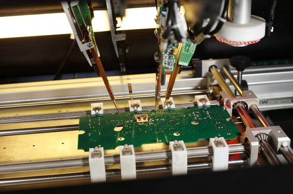
In-circuit test equipment consists of a number of elements:
· In circuit tester: The in circuit test system consists of a matrix of drivers and sensors that are used to set up and perform the measurements. There may be 1000 or more of these driver sensor points. These are normally taken to a large connector conveniently located on the system
· Fixture: The in-circuit test system connector interfaces with the second part of the tester - the fixture. In view of the variety of boards this will be designed specifically for a particular board, and acts as an interface between the board and the in circuit tester. It takes the connections for the driver sensor points and routes them directly to the relevant points on the board using a "bed of nails".
· Software: Software is written for each board type that can be tested. It instructs the test system what tests to perform, between what points and details of the pass / fail criteria.
4. What is the standard ICT machine?
In normal circumstances, this is the general test in this form of testing. However, they're standard because they offer elemental resistance, capacitance, and some device functionality.

5. What are the benefits of PCB ICT?
Although a costly fixture is required, ICT covers 100% testing so that all power and ground shorts are detected.
· ICT testing does power up testing and eliminates customer debug needs to almost ZERO.
· ICT does not take a very long time to perform, for example if flying probe takes 20 minutes or so, ICT for the same time might take a minute or so.
· Checks and detects shorts, opens, missing components, wrong value components, wrong polarities, defective components and current leakages in the circuitry.
· Highly reliable and comprehensive test catching all manufacturing defects, design faults, and flaws.
· Testing platform is available in Windows as well as UNIX, thus making it slightly universal for most testing needs.
· Test development interface and operating environment is based on standards for an open system with fast integration into an OEM customer’s existing processes.
Industry Category


