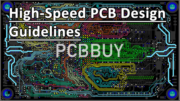
5 Essential Considerations of High Speed PCB Design Guidelines
By:PCBBUY 09/22/2021 10:00

Whenever you have signals on a PCB that have high-speed edge rates, they then become dependent on minute factors in the PCB layout. These signals can lose integrity and are affected by physical parameters such as board stack-up, impedance, loop area, general design, and package type.
In this passage, we will focus on the considerations of high speed PCB design, if you are interested in the high speed PCB design, please check and read the content we prepare for more information.
What are the 5 considerations about high speed PCB design?
1. Getting to know the importance of high speed PCB design
A good way to check whether you need to concern yourself with high speed board design guidelines is to layout your new device on a breadboard or a development board. If you can layout your new device on a bread board, and it works perfectly, then you can probably layout your board in any way you like and the finished PCB will still work.
However, high speed devices generally won’t work on a breadboard. If you can layout your peripherals on top of a development board, and the device works properly, then you can likely layout your new board however you like as long as you follow the stackup design in your development board.
2. Learn the standards of high speed PCB design
Before you route a single trace in the design, take some time to read an overview of the design requirements in your signaling standards. Make sure you understand the bus topology, length matching limits (if any), single-ended and differential impedance targets, noise margins/loss budgets, any off-die termination, and any other important requirements. Signaling standards information is available online and should be consulted if you’re working with any unfamiliar interfaces.

3. Pay attention to the challenges during high speed PCB design
The following section will highlight the main design challenges when it comes to designing high-speed PCBs
Tolerances
Since even minimal PCB characteristics can affect signal behavior, your manufacturer needs to have tight tolerances.
These are tolerances typically for things like controlled impedance traces, board Stackup, and capacitance, and also the overall length and width of marks.
Availability of high-speed material
Beyond certain speeds, you may start to require the use of unique PCB material if the signals get too fast.
Standard FR4 based fiberglass is not the best when it comes to designing high-speed boards. A few of the PCB materials used for high-speed designs are enhanced FR-4, Polyamide, PTFE.
Selecting the correct Layer Stackup
Another critical factor, especially in multi-layer boards, is selecting the right Layer Stackup, were to have a thick prepreg layer, where to have your power and ground planes, and also the separation between the sheets. All these factors, when chosen correctly, will improve signal integrity.
4. Learn about technologies of high speed PCB design
High-Speed Routing
A designer needs to know the rules for necessary routine when it comes to high-speed traces. It would include things such as not cutting ground planes and keeping trails short.

Routing traces with controlled impedance
Certain types of signals require impedance matching. These are usually in the order of 40-120 ohms. Characteristic impedance matched hints are Antennae and many differential pairs.
Length Matching Traces
High-speed memory busses and interface buses have many lines. These lines operate at very high frequency, and so the signals must arrive from the sending end to the receiving end at the same time.
5. Care about the circuitry routing of high speed PCB design
In high speed designs, the most direct trace path isn’t always going to be the routing solution that you need. For instance, you may need to route each connection in a daisy chain pattern, which will increase the total length of the routed net. At this point, you may need to adjust your component placement to better set up the high speed trace routing that you need. You will also need to route high speed transmission lines keeping the entire path of the signal in mind. It’s not just the trace from the driver pin of the IC to the resistor that you need to focus on. This is because a signal path continues through all components from driver to receiver; this is what is known as an extended net or xnet.
A lot of the trace routing that you will do in a high speed design will be the same as what you’ve always done. One possible difference is that of length requirements between traces. Some will have minimum length requirements,
Industry Category


