5 Essential Tips for Tenting Vias in PCB during PCB Manufacturing Process
By:PCBBUY 11/10/2021 09:17

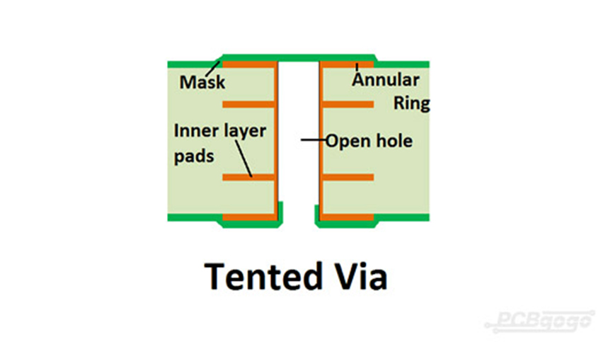
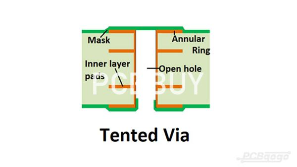
Tenting a via refers to covering via with soldermask to enclose or skin over the opening. A via is a hole drilled into the PCB that allows multiple layers on the PCB to be connected to each other. A non-tented via is just a via that is not covered with the soldermask layer. Leaving these vias exposed or covered has pros and cons depending on your design and manufacturing requirements.
Are you going to check for the information of tenting vias in PCB? In this passage, we are going to tell you everything about tenting vias in PCB. If you are curious about tenting vias in PCB, please check and read the content below for more.

1. Why to drill tenting vias in PCB?
Tenting vias does have its downsides. Since the LPI soldermask is a liquid, it has to “bridge” the gap over the via hole. This can cause the soldermask to not completely tent the via leaving a small hole. The small hole can provide a way for corrosive flux, moisture, and other chemicals to enter the via being trapped. This can enable the possibility of a failure of the via due to corrosion eating the copper via. This is less of an issue due to the popularity of no clean flux for SMT assembly but corrosive water clean flux is still prevalent in through hole assembly.
Leaving the vias exposed without soldermask does not mean the copper will be open to the environment. The exposed vias will be plated by the surface finish of the PCB. At MacroFab we use the ENIG finish which will cover the insides of exposed vias with gold, protecting the copper from corrosion and damage. For projects that are still in the prototyping phase it can be beneficial to have the vias exposed to be able to fix and reroute traces, and be used as impromptu test points.
2. What are the benefits of tenting vias in PCB?
First of all, provide the solder mask to the vias as the protection. It can prevent the copper traces from oxidizing and corroding just like the solder mask, and the solder mask does the same thing for the via. So tenting via can make an effect on preventing any damages to the PCB layers.

What’s more, it can reduce the number of conductive components that are exposed to external elements with the tenting method. As left exposed, the elements can reduce the integrity of the components and result in corrosion. As well as play a role in reducing the possibility of a short from happening from solder bridging.
There is no doubt that tenting vias are a cost-effective method, it can provide protection to the vias and the copper around it. And tenting a via with liquid photoimageable solder mask is the most cost-effective method of tenting.
3. When to choose tenting vias in PCB?
Whether or not you tent a via comes down to the design of the PCB and the size of the via. Typically, smaller vias are easier to fill or tent. When the via becomes 15mil in diameter, it ends up being too large for the tenting method.
Tenting vias providing extra protection for the hole and copper elements around it. If left exposed, the outside elements can cause the copper to corrode and damage the PCB. With the tenting method being cost-effective as well, the advantages of tenting a via outweigh the disadvantages. For via-in-pad technology, non-conductive via fill should be considered.
4. What is the process of tending via in PCB manufacturing?
Vias can be very negligible in size, but they are crucial parts of a printed circuit board (PCB). Vias are used to interconnect the copper traces present on different layers of a multi-layered PCB. You will never find any component lead passing through the hole of a via. There are different types of vias, and drilling holes on the PCB make all of them.
A via may be tented or left exposed — a tenting of a via means that solder mask has been used to cover the via over the hole in the shape of a tent or a skin. Earlier, manufacturers had to face difficulty in tenting the vias as they used liquid photo-imageable (LPI) solder mask. But with the introduction of the dry film solder mask, the process has become much more comfortable.
Tenting a PCB brings down the number of exposed conductive pads and reduces the chances of shorts arising from solder bridging. It also protects the vias from corrosion and external elements. When dealing with SMT pads, tenting is useful to lessen past migration from the SMD elements when the vias are designed at the end of places. Tenting is also ideal for vias located close to SMT pads, reducing the chances of short that occur during reflow. Sometimes, the tented via is again given a coat of solder mask.

5. What are the differences of tenting vias VS plugged vias?
Tenting Vias is a process where the solder mask is used to cover the vias. Different procedures of tenting can be used, such as screen coating, spray, and curtain. But the methods may not be enough to provide a complete tenting of the via. For example, squirt and specific strategies may not suffice to wrap the via on both sides. The process of screen coating also has some limitations by hole size and board thickness.
Plugged vias are useful in many scenarios, such as BGA design, where the vias are generally placed very close to the SMD pads. In such scenarios, plugged vias come to the rescue. While fabrication, steps ensure that the masked plugging or the non-conductive fills form a complete seal and tents the annular ring. The process guarantees that the vias are 100% tented and filled.
While plugging, the mask clearance is first removed from the via. Then the holes are filled based on the design parameters of the PCB. The via plugging is carried out based on the standards developed by the IPC. You have got the hang of raw via tenting and plugging concepts. Now we will take the discussion further with solder-filled vias in the next chapter.
Industry Category


