5 Important Factors of High Voltage PCB Layout Guidelines
By:PCBBUY 06/24/2022 10:16

When creating a PCB for high voltage DC bias, standards and precautions become much more stringent. High voltage PCB materials and design for arc prevention ensure the final product is safe and functional. Avoid increased costs and danger by keeping these PCB materials and design tips in mind.
Are going to search for more information about high voltage PCB layout? If you are curious about high voltage PCB layout, please check and read the content below for more professional knowledge.

What are the features of high voltage PCB?
Isolation Slots and cut-outs
Most high voltage boards require isolation slots and board cut-outs near any board section, which carries high voltage.
In many consumer devices like chargers and power supplies, these slots and board cut-outs are mandatory to pass certain safety standards. These features add an extra layer of safety and would help in high humidity environments and cases where contamination is likely.
Isolation slots and cut-outs will usually have to define on a mechanical layer of the board.
Board Material
Standard FR-4 is not a good material for high voltage boards as it has low dielectric strength.
Whenever the cost is not a constraint, it is better to go for a board material with a higher dielectric strength. Some of the high voltage rated materials are:
1.BT Epoxy
2.Polyimide
3.Isola
Board Finishing
The most underlooked and important factor when it comes to high voltage PCBs is the board finishing. It mainly includes the surface finish on the pads and any exposed traces. Mainly the finished board should have a smooth finish free of any bumps and should be even along the entire surface.
Any imperfections on the high voltage pads like sharp points can result in a high electric field region, which can then cause arcing.

What are the best design practices of high voltage PCB?
Time and again, manufacturers receive feedback from PCB users on high voltage boards. This information helps in creating best practices that can reduce the chances of errors in production.
Routing
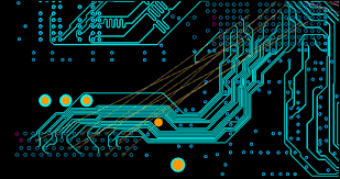
Routing best practices are essential to maintain when designing a high voltage PCB. Ideally, the designer maintains clearance between traces that have a high voltage difference in between. Moreover, it would be best to avoid any sharp edges because they can act as areas of high concentration of electric field. In the internal layers of the board, it’s crucial to avoid running high voltage traces as well.
Internal Layers
It’s also vital to make a multi-layer PCB with a medium voltage on each layer. Filling the spaces between the layers requires caution. The thickness of each separation between layers must be .005” in order to maintain a balance in the overall PCB design. In high voltage PCBs, any voids or useless gaps disturb the dielectric value.
Polygon Planes
You should also consider increasing the polygon plane clearance until it touches a safe value in all high voltage PCBs. Internal planes in a multi-layer PCB should have the appropriate separation and a high voltage. This enables the smooth passing of the current without disrupting the other elements on the board.
EMI
You may have heard about high voltage PCBs emitting a disturbance on a wide spectrum. To minimize this issue, you can shield the high voltage items after potting with the help of a metal sheet. A small loop area in the ground plane can greatly help in minimizing the disturbances.
Industry Category


