5 Important Factors of PCB Stack Up Analysis and Design
By:PCBBUY 03/05/2022 10:21

A stackup is the arrangement of layers of copper and insulators that make up a PCB before designing the final layout of the board. Managing a good stackup is not exactly easy and companies that make multilayer printed circuits such as Proto-Electronics, a European platform dedicated to the rapid prototyping of SMT printed circuits and cross-section components, for professionals, must be at the forefront.
If you are searching for the basic information about PCB stack up, please check and read the content below for more professional knowledge.
What are the different layers in a multilayer PCB?
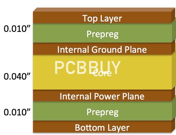
A stack-up primarily consists of metal foil, prepreg, and copper-clad laminate (core).
· Metal foil: Copper is the most commonly used metal foil in PCB construction.
· Prepreg: It is an interwoven glass cloth impregnated in epoxy resin. The resin is left semi-cured.
· Copper-clad laminate: Single or multiple plies of prepreg bonded together along with the top and bottom copper foil makes a copper-clad laminate. This is also known as the core.
What are the advantages of standard PCB stackup?
Having multiple layers (see figure 1) increases the board's ability to distribute energy, reduces cross-interference, eliminates electromagnetic interference and supports high-speed signals. While a stackup level allows you to get multiple electronic circuits on a single board through the various layers of PCB board, the structure of the PCB stackup design provides many other advantages:
· A stack of PCB layers can help minimize the circuit vulnerability to external noise, as well as minimize radiation and decrease impedance and crosstalk problems on high-speed systems;
· Good PCB stacking can also contribute to efficient and low-cost final production;
· A correct stack of PCB layers can improve the electromagnetic compatibility of the project.
How to process PCB stack up design?
In order to make the best decisions when designing a PCB stackup, it is useful to understand how multilayer PCBs are manufactured. There are a number of methods used to fabricate multilayer PCBs. The most common and most economical is called foil lamination. Figure 3.1 is a pictorial of a typical six-layer PCB. Notice that there are three basic components in the stackup. These are: sheets of copper foil in the top and bottom of the stackup, sheets of prepreg and sheets of laminate.

The outer layers are always solid sheets of copper foil until after the stackup has been laminated and drilled. The reason for this is to provide a path for the plating current used to plate copper in the drilled holes used as vias and component leads. The material known as prepreg or B stage is woven fiberglass cloth that has been coated with the resin system chosen for a particular design. This resin has been only partially cured and will serve as the “glue” when the stackup goes through lamination. The component laminate is the same glass/resin material as the prepreg. It has a layer of copper in each side that is bonded to the glass/laminate in a press that cures the resin, resulting in a rigid piece of material called laminate. The inner signal and plane layers will be etched on these pieces of laminate, two at a time.
Why to process PCB stack up design?
Most circuit boards today have some elements of high-speed circuitry involved with them, meaning that the signal integrity of the board will be a primary consideration. High-speed transmission lines usually require an adjacent ground plane if routed on the board’s surface in what is known as a microstrip layer configuration. If the high-speed transmission lines are routed on internal layers sandwiched between two ground planes, this is known instead as a stripline configuration. These layer configurations will provide an excellent reference plane for clear signal return paths, eliminating the most prolific cause of electromagnetic interference (EMI) in circuit boards. The ground planes also help shield the high-speed transmission lines from incoming interference and radiate their own interference.
Sensitive high-speed signals require added space to protect them from other forms of noise and interference:

Trace separation
When high-speed traces are too close to each other, one signal may overwhelm the other and impose its signal characteristics on it instead. This imposition may cause the victim signal to mimic the aggressor signal instead of producing its expected behavior.
Impedance matching
Going through different areas of the board can change the characteristic impedance on high-speed signals. This change can cause signal reflections which could distort the original signal and interrupt the intended function of the circuit.
Circuitry isolation
Power circuitry and analog circuitry can all create their own brand of noise, impacting the regular operation of digital circuitry. It is imperative to keep the trace routing of these different areas isolated from each other.
The board’s power delivery network (PDN) is another area that can suffer if it isn’t designed correctly into the board layer stackup. There must be enough layers to support the multiple power nets in a high-speed design so that power is delivered cleanly throughout the board. High-speed digital devices have fast switching speeds, which may not always return to their low state. This “ground bounce” effect can cause the ground reference level to rise in the board, creating false states and corrupting the signals sent and received in the devices. One way to counter this problem is to configure the board with large ground planes and make sure each ground pin of the high-speed devices is directly connected.
Industry Category


