What is PCB Drilling: 5 Instructions of Castellated Holes in PCB?
By:PCBBUY 10/20/2021 09:36

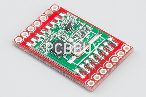
Castellated holes are plated through holes or vias located in the edges of a printed circuit board. Castellated holes are cut through to form a series of half holes. These half holes serve as pads intended to create a link between the module board and the board that it will be soldered onto.
In this passage, you will get everything about the information of castellated holes on PCB. If you are interested in castellated holes on PCB, please check and read this passage for more professional knowledge.
1. What is the basic introduction of castellated holes on PCB?
Castellated holes are indentations created on the edges of a PCB board. They are also called castellated holes. These holes are in the form of semi-plated holes. These holes help in the mounting of one PCB board on top of another. It makes the assembly process much more convenient. However, based on the application, these holes may take the form of a portion of a broken circle. These castellated holes help provide proper alignment between the two boards.
Thus, it helps the appropriate soldering of boards. The castellated holes assist the mounting process, namely board-to-board soldering. You can use castellations in several PCB modules, be it a Wi-Fi module or a Bluetooth module. These modules can be mounted together while soldering, though they are independent parts. These castellated holes connect two PCBs directly.
2. How to manufacture castellated holes PCB?
Once you’ve placed the castellated holes onto your PCB, how do you get the bare board fabricated? The goal here is to ensure high quality and yield in a standard process, but castellated holes do not seem to fit into the standard PCB fabrication process. Your fabricator can help you ensure your design will pass through fabrication by modifying the Gerbers to indicate drill hits and required plating along the board edge. This normally requires the following Gerbers (X2 format):
· Copper layers (GTL and GBL)
· Solder mask openings defined on both board surfaces (GTS and GBS)
· Drill files (TXT/DRL)
Some would say that the natural alternative to castellated holes is to just use solder pads to mount the module to your main board, just like any other SMD component. The main problem with this is the potential for contamination; the pad array on the carrier board can trap exhaust from some fluxes during reflow soldering. Another possibility is that excessive solder paste along the pad array lifts the module. This is similar to what can happen with SMD ICs that have a large ground pad in the center of the component.

3. What are the applications of castellated holes PCB?
· Castellated PCBs can be used as breakout boards for a particular portion of the larger PCB.
· These holes give ease to change the Pin layout of the component as per the user requirement.
· Integrated modules can be produced on a single PCB board using castellation, which can be used further into another assembly during production.
· PCBs with castellated holes can be mounted easily to another PCB during final production.
· They are used to combine two boards to validate the solder joint quality.
· They are used for breakout boards or small modules like Wi-Fi modules.
· Castellated holes also help to create wireless PCB to PCB links.
4. What are the specific considerations of castellated holes PCB?
· Half hole printed circuit board
· Cost-effective, high quality
· PCB OEM & ODM are available
· ISO9001, UL, RoHS certificated
5. How to design PCB castellated holes?
Castellated Holes (a.k.a. Plated Half Holes, Castellations, ... ) are a series of Plated Through Holes or Vias placed on the edges of the PCB and allow you to transform your PCB into a surface mounted sub-assembly. When cutting the board at the end of the manufacturing process, only a half of each plated hole remains in the PCB. These Plated Half Holes now serve as pads to solder the sub-assembly to the surface of the motherboard.

Integrating Castellated Holes to your PCB is very easy. Just make sure to pay attention to the following points:
· Place the center point of every castellated hole exactly on the edge/ board outline of your PCB. It is important that these holes are plated-through. They must be included in the drills-layer.
· Always use the top and/or bottom edges as locations for your holes! Do not use the vertical edges (left and right), because they are predominantly used for our bridges to hold the PCB in place. See also our article about Bridges and Frames.
· The copper-layer should have pads while the soldermask-layer should have openings.
Minimal diameter of castellated holes: 1.0 mm (0.04 in)
Industry Category


