5 Key Points of PCB DIP Soldering Process in PCB Manufacturing
By:PCBBUY 10/21/2021 09:25

Manual immersion tin and semi-automatic/fully automatic welding equipment have been developed. We will step through this process in this article. If you are going to learn more information of PCB DIP soldering, please check and read the content in the article for more professional knowledge.
1. What are the benefits of PCB DIP soldering?
Then certain essential functions allow you to use these displays for residential and commercial advertisement activities,
· High contrast and luminosity
· Broad angle of view
· Image playback and visuals, motion shown
· Rate the number of times an ad has been seen
· Online management and planning
· Daytime and range do not influence workload
The operating capability is not affected by the time of year, weather, and temperature change
The stability and long life of the LED show for up to 10 years is one of the biggest advantages. In addition, the show would not stop running, except though part of it is damaged. The defective cluster remains unnoticed.

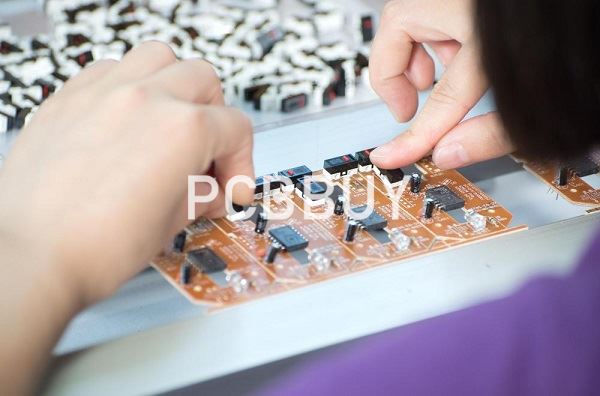
2. What are the preparations before of PCB DIP soldering?
First Article Inspection
We will cross check and record all the supplied components’ quantity, item number, dimension, cathode direction, component silkscreen number, value, etc.
Components outline processing
Some components outline should be processed ahead of time because of their own design or for the PCB DIP soldering requirements and the whole PCB plan.
Requests. The horizontal witch of the processed pins should be the same as the locating holes, the tolerance should be < 5%, the silkscreen upward.
Components management
Preparation before DIP soldering: Every operator should follow team leader’s arrangement, prepare their WI content in their own station and receive all the components which match the WI completely. Put the received components into the part box and mark them well, including the defect parts if there is. Check if there is any cathode components, and compare with the WI picture, should be familiar with the part appearance and find out the pin position.
3. What are the differences of DIP and SMT?
SMT only assemble no pins components such as QFN,DFN,BGA package components or short pins components on the PCB surface. It need to print solder paste on the PCB firstly, than use the SMT machine to solder the components, finally via reflow soldering to fix components on PCB.

While DIP is solder the through hole package components, and via wave soldering or manual soldering to fix components on PCB.
SMT and DIP are all part of the PCB Assembly work, but not all the PCBA companies have good SMT and DIP capability, and the PCB soldering quality are not the same. If you cooperate with a new PCBA factory, I suggest you firstly visit the factory to check the assembly technology, production equipment and so on.
4. What is the process of DIP and SMT?
Dip soldering is accomplished by submerging parts to be joined into a molten solder bath. Thus, all components surfaces are coated with filler metal. Solders have low surface tension and high wetting capability. There are many types of solders, each used for different applications:
· Lead–silver is used for strength at higher-than-room temperature.
· Tin–lead is used as a general-purpose solder
· Tin–zinc is used for aluminium
· Cadmium–silver is used for strength at high temperatures
· Zinc–aluminium is used for aluminium and corrosion resistance
· Tin–silver and tin–bismuth are used for electronics.
Because of the toxicity of lead, lead-free solders are being developed and more widely used. The molten bath can be any suitable filler metal, but the selection is usually confined to the lower melting point elements. The most common dip soldering operations use zinc-aluminum and tin-lead solders.
5. What are the features of PCB DIP process?
DIP is one of the basic components of electronic components. It is called dual in-line packaging technology, which refers to the integrated circuit chip packaged in the dual in-line form, which is also used in most small and medium-sized integrated circuits. The number of pins generally does not exceed 100.

A CPU chip with DIP packaging technology has two rows of pins, which need to be inserted into a chip socket with a DIP structure. Of course, it can also be directly inserted into a circuit board with the same number of solder holes and geometric arrangement for soldering. DIP packaging technology should be especially careful when plugging and unplugging from the chip socket to avoid damage to the pins.
Features: multilayer ceramic dual in-line DIP, single-layer ceramic dual in-line DIP, lead frame DIP (including glass ceramic sealing type, plastic encapsulation structure type, ceramic low-melting glass packaging type) and so on.
Industry Category


