5 Main Aspects of PCB Copper Distribution in PCB Manufacturing Process
By:PCBBUY 11/24/2021 09:10

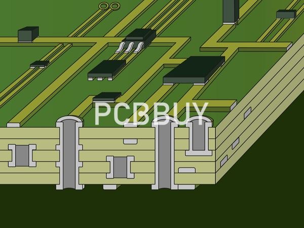
The manufacturing of the copper traces of your board, whether on the surface or for internal layers, is done by etching, one of the major PCB manufacturing steps. Layer fabrication begins with a laminate sheet that is completely covered by copper. Etching is the process of removing excess copper from traces and other areas, such as component pads and annular rings for vias, using an ammonia-based solution.
If you are looking for the knowledge of PCB copper, you can check and read this passage for more information about PCB copper. Don’t miss the useful content for your PCB area to study. Let’s check it!
What is the significance of copper balance in PCB manufacturing?
Copper is an electric conductor, which is used in various forms in the PCB. The elements like traces, core, layers, and final coating consist of copper as the main component. If copper coverage is inconsistent between the layer stack-up, it can lead to issues like bows and twists, warpage, etc.
Let us discuss the problems that need to be avoided by the proper copper balance in PCB fabrication.
· Bows: Inconsistent copper coverage causes cylindrical or spherical curvature on the PCB layer, this is known as the bow. The bow causes tension or compression on the surface of PCB according to the direction of the bend. This can lead to the inconsistent circulation of electric current across the board.
· Twists: If one of the corners of the PCB is not parallel to the others, the surface lift from one end of the diagonal and surface depth on the other ends creates a twisting effect. The twist causes stress in the PCB layers.
· Warpage: Inconsistent layering of copper on the PCB leads to warpage. The warpage is also known as the potato chip effect. This may cause saturation of electric current and uninformed distribution of current across the board. It can also interrupt the function of traces and connection leads of mounted components.
How is Copper Used in PCBs?
Copper has several uses in PCBs, from the copper-clad laminate to the traces. Copper is vital for PCBs to work appropriately.

What is PCB Trace?
A PCB trace is what it sounds like, a path for the circuit to follow. The trace includes the network of copper, wiring, and insulation, as well as the fuses and the components that are used on the board.
The easiest way to understand a trace is to think of it as a road or bridge. To accommodate vehicles, the trace needs to be wide enough to hold at least two of them. It needs to be thick enough not to collapse under pressure. They also need to be made of materials that will withstand the weight of the vehicles that travel on it. But, traces do all of this to a much smaller degree to move electricity rather than automobiles.
Components of PCB Trace
There are several components that make up the PCB trace. They have various jobs that need to be done for the board to do its job adequately. Copper has to be used to help the traces do their jobs, and without the PCB, we would not have any electrical devices. Imagine a world without smartphones, laptops, coffee makers, and automobiles. That is what we would have if PCBs did not use copper.
What is the standard PCB copper thickness?
The most common unit of measure for the copper thickness on a printed circuit board is ounces (oz). But most of people have no idea about how thick is it. It's the finished thickness when 1 oz copper is pressed flat and spread evenly over a one square foot area, which equals 1.37 mils. Of course not everyone thinks in mils so you can convert into your preferred unit of measure with our unit conversion tool.

Most printed circuit boards are constructed with 1 oz copper thickness. In PCB manufacturing, if customers do not offer specific specs, we will assume 1 oz when quoting and building the design. If customers have decided that the design requires more current than 1 oz can carry, it would better to consider increasing the copper thickness or increasing the width of your traces. Of course the thicker the copper the higher the cost, but there are certainly times if it is necessary. The cost increase is not only due to the raw material costs but processing thicker copper weights takes more time and is a little trickier to do.
What are the materials of copper laminate in PCB?
Copper Foil
Copper foil is a cathodic electrolytic material deposited on a thin, continuous layer of metal foil on the base of the circuit board. It is easily bonded to an insulating layer, accepting a printed protective layer, and corroded to form a circuit pattern.
Prepreg
A prepreg (from pre-impregnated) is fiberglass impregnated with resin. The resin is pre-dried, but not hardened, so that when it is heated, it flows, sticks, and is completely immersed. Prepreg are thus fiberglass strengthened by an adhesive layer (similar to FR4 material). The name of each prepreg derives from the type of fiberglass used.
The prepreg types of different suppliers vary in thickness; in addition there are the versions "SR" Standard Resin, "MR" Medium Resin "and" HR "High Resin, depending on the resin content. The best possible material is used depending on the desired final thickness, layer structure or impedance. The mentioned thicknesses are thus to be considered only as examples.
Industry Category


