5 Main Factors of Standard PCB Stackup Thickness in Manufacturing Process
By:PCBBUY 11/06/2021 10:36

A PCB stackup refers to the arrangement of copper and insulating layers that make up a PCB. These layers are arranged in a way to get multiple printed circuit boards on the same device. At their most basic, multilayer PCBs consist of at least three conductive layers. The bottom layer is synthesized with the insulation board, and each circuit board layer is connected to the next.
Are you going to learn more about PCB stackup? In this passage, you will get everything about standard PCB stackup, please check and read the content below for more.
1. What are the advantages of standard PCB stackup?
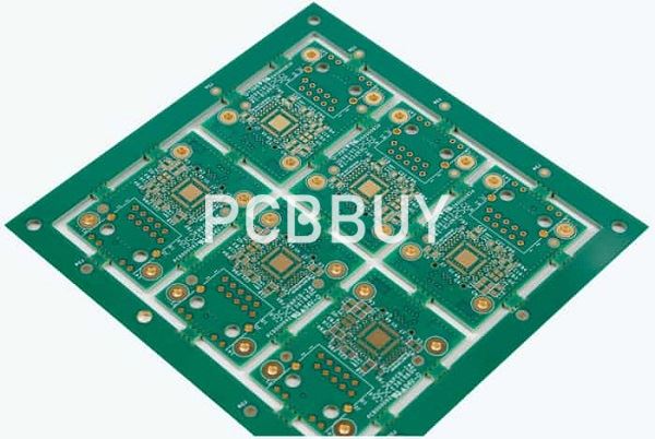
Having multiple layers (see figure 1) increases the board's ability to distribute energy, reduces cross-interference, eliminates electromagnetic interference and supports high-speed signals. While a stackup level allows you to get multiple electronic circuits on a single board through the various layers of PCB board, the structure of the PCB stackup design provides many other advantages:
· A stack of PCB layers can help minimize the circuit vulnerability to external noise, as well as minimize radiation and decrease impedance and crosstalk problems on high-speed systems;
· Good PCB stacking can also contribute to efficient and low-cost final production;
· A correct stack of PCB layers can improve the electromagnetic compatibility of the project.
2. What is the perspective of standard PCB stackup design?
Regardless of the number of layers that comprise your board design, specifications for pad spacing, clearances, trace widths, copper weights and drill hole sizes must be tailored to your contract manufacturer (CM). If your design requires multiple layers, you will need to consider additional design for manufacturing (DFM) specifications for signal, power and ground routing through vias, as well as the PCB stackup. These additions entail incorporating verticality into your design perspective.
The PCB stackup design perspective that includes both vertical and horizontal considerations is a three-dimensional approach that significantly impacts board fabrication and PCB assembly. For fabrication, the number of layers, their arrangement or stackup and type of material must be determined. These choices require coordination between thicknesses restrictions; material parameters; such as dielectric constant, the coefficient of thermal expansion and electrical strength, signal type isolation and drill hole options. For PCB assembly, via routing options and their effect on the soldering process are of great importance. The capabilities of your CM limit the choices for the vertical aspect of your design.

3. What are the differences between standard stackup and HDI stackup?
There are fundamental differences between standard stackup and HDI stackup. For standard stackup, there are factors to take note of including: progression of layers, the quantity of the layers, circuit's frequency, and requirements regarding emission. Other parameters related to standard stackup include: the space between the layers and shielded or unshielded area.
Of great importance still, are the design rules that are important for standard stackup. The rules include: maintaining the space between the layers of signals and using large cores to evade EMC issues. Another thing that is significant to note is the benefit of standard stackup, which is guarding of inner layers using the planes on the exterior layers. The disadvantage is the lessening in the ground plane as a result of the presence of component mounting pads, specifically on a PCB with high density.
HDI stackup is the technology that is transforming the manufacturing and design of multiplayer PCB. Unlike the standard stack up, HDI stackup offers more design choices. Additionally, if you would like to have a simplified design for complex boards, HDI stackup is the right choice. The factors that determine stack up include: the quantity of signal layers and the quantity of ground and power layers. An important thing to take note of is that the layers should have a symmetrical arrangement. The fact that HDI does not need complicated architectures is a big plus for designers.

4. What is the high-speed PCB stackup?
Many years ago, you could design many printed circuit boards without much thought to signal integrity because the signal speeds of the boards weren’t fast enough to warrant any concern. That is no longer the case, however, as even an average PCB design now needs signal integrity consideration.
Designers must allow for the space that will be needed for controlled impedance routing and to guard against congested layouts that can create crosstalk. High-speed transmission signals need enough room to be routed in such a way as to avoid using vias, and measured trace lengths and trace length matching all need additional room, as well. All of these extra routing requirements may result in your circuit board needing additional layers with their stackup configuration precisely planned.
5. How to determine the multilayer PCB stackup?
Having multiple layers (see figure 1) increases the board's ability to distribute energy, reduces cross-interference, eliminates electromagnetic interference and supports high-speed signals. While a stackup level allows you to get multiple electronic circuits on a single board through the various layers of PCB board, the structure of the PCB stackup design provides many other advantages:
· A stack of PCB layers can help minimize the circuit vulnerability to external noise, as well as minimize radiation and decrease impedance and crosstalk problems on high-speed systems;
· Good PCB stacking can also contribute to efficient and low-cost final production;
· A correct stack of PCB layers can improve the electromagnetic compatibility of the project.
Industry Category


