5 Main Tips of Ceramic PCB Manufacturing Process for Beginners
By:PCBBUY 10/26/2021 09:09

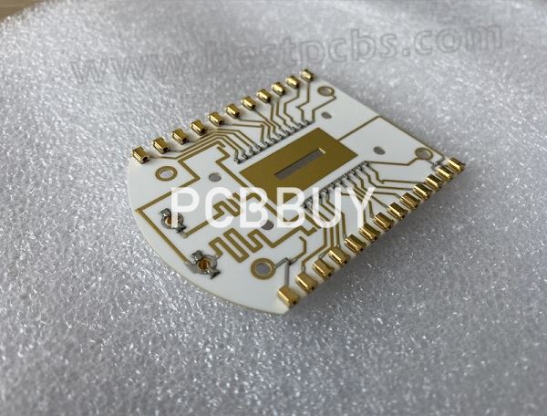
The word ceramic refers to a group of materials with chemical structures and physical qualities that are similar. Ceramic printed circuit boards (PCBs) have a ceramic base material made up of highly thermally conductive materials, including alumina, aluminum nitride, and beryllium oxide. Ceramic printed circuit boards have proven instrumental in the creation of smaller electronic devices.
Are you interested in ceramic PCB manufacturing? Do you want to learn more about ceramic PCB? If you are going to get more information about ceramic PCB manufacturing, please check and read the content we prepare below.
1. What are the advantages of ceramic PCB?
Besides its enviable thermal properties and low CTE, ceramic PCBs come with a few other benefits. Review some of their advantages below:
· Safe operation in temperatures up to 350 degrees Celsius
· Simple implementation of high-density tracing
· Exceptional high-frequency performance
· Versatile packaging, with an option to come in hermetic packages to prevent water absorption
· Tough chemical erosion resistance
2. What are the main types of ceramic PCB?
High temperature
As you know, high temperature may be the most popular types pf ceramic. In general, The ceramic PCB designed for high temperatures is often regarded as high temperature co-fired ceramic (HTCC) circuit, which is made up of raw ceramics with solvent, mixing adhesive, plasticizer, lubricant as well as aluminum oxide.
First of all, it fabricates with the raw ceramic material, secondly coat the material, and then carry out the circuit tracing on tungsten or molybdenum metals. Finally, if the circuit tracing is achieved, it can bake the boards between 1600 and 1700 degrees Celsius for up to 48 hours after lamination. All HTCC baking is done in a gaseous environment, such as in hydrogen gas.
Thick film ceramic
Thick film ceramic PCB, the thickness of its conductor layer may exceed 10 microns, but not more than 13 microns. In general, the conductor layer is printing the silver or gold palladium on the surface of ceramic PCB. That is to say, thick film ceramic PCB includes gold and dielectric pastes, which is done on a ceramic base material, and the pastes and backed at a temperature of 1000 degrees Celsius or below after working. So the thick film ceramic PCB is widely used for most PCB manufacturers because of the high cost of gold conductor paste.
The main advantage of thick film ceramic PCB over traditional PCB is that thick film ceramic can protect copper from oxidizing. So a ceramic PCB manufacturer can put interchangeable conductors, semi-conductors, conductors, electric capacitors, or resistors on the ceramic board. After achieving the process of printing and high-temperature sintering, all the components on the board can be laser-trimmed to their desired values.

3. What is the manufacturing process of ceramic PCB?
Traditional ceramic substrate manufacturing methods can be divided into four types: HTCC, LTCC, DBC, and DPC.
· The HTCC (high temperature co-fired) preparation method requires a temperature above 1300°C, but due to the choice of the electrode, the preparation cost is quite expensive.
· The LTCC (low temperature co-firing) requires a calcination process of about 850°C, but circuit precision is poor, and the thermal conductivity is low.
· The DBC requires formingan alloy between the copper foil and the ceramic, and the calcination temperature needs to be strictly controlled within the temperature range of 1065-1085°C. Because the DBC requires the thickness of the copper foil, generally, it cannot be less than 150-300 microns. Therefore, the wire width to depth ratio of such ceramic circuit boards is limited.
· The preparation methods of DPC include vacuum coating, wet coating, exposure and development, etching, and other process links, so the price of its products is relatively high. In addition, in terms of shape processing, DPC ceramic plates need to be laser cut. Traditional drilling and milling machines and punching machines cannot accurately process them, so the bonding force and line width are more precise.
4. What are the properties of ceramic PCB?
Compared with traditional PCBs whose substrate materials are epoxy glass fiber, polyimide, polystyrene and phenolic resin, ceramic PCBs feature the following properties:
• Excellent thermal conductivity
• Chemical erosion resistant
• Agreeable mechanical intensity
• Compatible with CTE of components
• Easy to implement high-density tracing.
Due to increasingly multiple functions, miniaturization and high speed of electronic devices and upsizing of IC, more rigorous requirement has to be set to ceramic PCBs in terms of CTE, thermal conductivity, loss, dielectric constant and tape resistance. It can be estimated that ceramic PCBs will be increasingly more called for with aluminum nitride, mullite and glass ceramic as substrate material.

5. What are the applications of ceramic PCB?
Multi-layer interconnect board
To be compatible with miniaturization of electronic products, ceramic PCBs are able to hold more components within the same board area, which adds more possibilities for ceramic PCBs in the applications of multi-layer interconnect board.
Digital PCB
AGC Company from Japan took advantage of LTCC PCBs to produce analog/digital PCB boards so that parasitic capacitance can be reduced by approximately nine tenths. It not only effectively overcomes crosstalk interference of circuit tracing, but also reduces volume and weight of circuit.
Industry Category


