5 Nice Guidelines of Bluetooth Circuit Board Design to Improve Manufacturing Process
By:PCBBUY 11/03/2021 09:13

Bluetooth is a form of communication that utilizes radio frequency to connect with different devices. It can operate at 2.4 GHz frequency and is similar to the other wireless communication forms, such as Wi-Fi. Bluetooth boards exist in the devices and devices we use every day without careful consideration. Anything that uses a wireless connection can be using Bluetooth radio frequencies even without your knowledge.
In this passage, we are going to provide all the details about Bluetooth PCB design. If you are interested in Bluetooth PCB design guidelines, please check and read the content below for more information.
1. What are the applications of Bluetooth PCB?
A variety of applications utilize Bluetooth, including:
· Beacons used in shopping malls
· Eddystone frames for industrial sensing applications
· Headsets and audio/stereo products
· Remote peripheral devices such as video game controller or computer mice/keyboards
· Home automation systems
· Wireless consumer electronics applications including cameras, printers and phones
Each application incorporates the same common Bluetooth technology, but utilizes it differently and depending on the connection type, it’s up to the design engineer to incorporate basic principles to optimize signal integrity and overall device effectiveness.
2. What are the components for Bluetooth PCB?
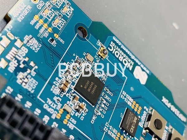
A Bluetooth circuit board also contains a minimum of 2 inductors, which can fine-tune the antenna's impedance to improve the reception and sending of information. The modules have 4 IO pins: the State, Enabled, communication, and power supply options. You can also find multiple resistors, diodes, and capacitors placed on the Bluetooth circuit board.
Apart from the above components, other parts such as chips, voltage regulators, and the crystal-based clock can also be found. The Bluetooth circuit board requires careful attention while assembling, especially with the antennae for its proper functioning.
It is what a Bluetooth circuit board looks like. Like we have already said, Bluetooth circuit boards are found within Bluetooth-enabled devices. In the next chapter, we will explore some of the practical applications of Bluetooth circuit boards.
3. What are the recent technologies of Bluetooth PCB?
Bluetooth, like all technology, is steadily evolving as the demand for it increases. Also, currently, the newest Bluetooth standard is version 5.0, which began in 2016. Like cellular transmission standards increase, so does Bluetooth technology. Furthermore, the technology, as a whole, uses classifications to signify the wireless range of the device. More specifically, there are three classifications of Bluetooth, and they are as follows;
Class 1 signifies a range of 328 feet (maximum). For example, laptops and PCs.
Class 2 indicates a range of 33 feet (maximum), and it is the most common class on the market — for example, smart phones and Bluetooth headphones.
Class 3 designates a range of approximately 3.3 feet (maximum) — for example, small devices like an ECG (electrocardiogram) stress test wireless medical device.

4. How to design low energy for Bluetooth PCB?
Designing a new Bluetooth product, or any wireless product, can be somewhat challenging for the inexperienced. This is primarily due to the complexity of the PCB layout for the RF (radio frequency) section. Fortunately, in BLE microchips, most of the RF circuitry is internal, so you don't need to worry about much more than the layout for the antenna.
Bluetooth Low Energy is a very popular open wireless standard for short-range communication. The range is typically about 50 feet, although this can be significantly increased with the use of a range extender circuit that either increases the receiver sensitivity, increases the transmission power, or both.
As the name implies, Bluetooth LE is a low-energy version of "classic" Bluetooth and thus is more appropriate for ultra-small devices powered by a single watch battery. BLE is the primary wireless technology for Internet of Things (IoT) products.
5. How to design the antenna for Bluetooth PCB?
hen not using a pre-certified BLE module with a built-in antenna, one of the most critical aspects of the design will be the antenna and the transmission line between the antenna and the transceiver.
There are two choices for the BLE antenna: a chip antenna or a PCB-trace antenna. A chip antenna has the advantages of smaller size and simplified tuning. A trace antenna is designed into the PCB itself. The main advantage of a trace antenna is the reduced unit cost. In fact, because the antenna is just a trace on the PCB, the antenna is essentially free.
However, chip antennas are rather cheap, so in most cases a chip antenna is a better choice—at least initially.
This design uses a chip antenna from Pulse Electronics. Once your product achieves large production volumes, you may want to replace the chip antenna with a PCB-trace antenna in order to reduce your unit cost and improve the profit margin.
PCB trace antennas tend to be more problematic to tune, however, and many times they require several PCB revisions in order to optimize tuning. Modifications to the PCB will also have a more pronounced impact on a trace antenna's tuning versus that of a chip antenna.
Industry Category


