5 PCB Common Faults & How to Solve PCB Problem?
By:PCBBUY 09/11/2021 09:47

During the layout and manufacturing process of PCB, there will be many problems and challenges. Indeed, PCB defects may not be as problematic for prototype designs or smaller volumes boards. It may be frustrating to make a few manual corrections here and there, but those alterations can be more efficient than redesigning the board. For larger production runs, however, this is not the case.
In this passage, follow us and check the content below. You will learn everything about PCB common faults. If you are curious about the topic, please read the content we prepare for more knowledge.
What are the 5 PCB common faults?
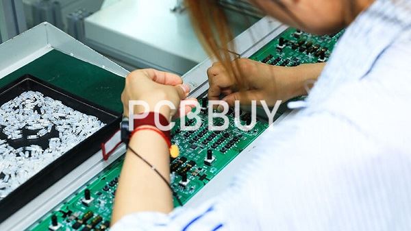
Soldering fault
The bulk of printed circuit board defects can be traced back to a soldering issue. Soldering is a technical skill that becomes even more difficult when dealing with the extremely small components on a printed circuit board. Soldering defects can be minimized both during the design process, and during the soldering process. Some of the most common soldering defects include:
Open joints, sometimes called “dry joints,” occur when the solder doesn’t bond correctly with the point of contact, typically the pad. Open joints do not always cause your circuit to fail, since there may be solder there that makes poor or occasional contact. Open joints are caused by physical movement or bending, incorrect solder temperature, design or manufacturing errors, as well as impact and shifting during use or transport.
Temperature fault
Printed circuit boards are affected by temperature, both in storage, and when they are installed in components. Extreme temperatures or large temperature fluctuations may cause components or joints to break or fail. Many people take the maximum or minimum safe temperature into consideration, without thinking about the fluctuations in temperature that may occur either during operation or in storage. Temperature fluctuations can cause expansion and contraction to take place too quickly, causing premature failure of the printed circuit board.
Plating fault
Holes carry electricity from one side of the board to the other. Plating of the hole wall during manufacture. During this, By establishing the electrical conductivity from the top in the endplate portion depositing copper.
If the copper deposition is incorrect, it will create plating voids, leaving gaps in the wall with no copper coating. It could happen due to air bubbles, contamination in the holes, contaminated materials, and other similar reasons. You can prevent this from happening by following the manufacturer’s direction and cleaning the equipment as instructed.

Electromagnetic Compatibility fault
Electromagnetic interference (EMI) and electromagnetic compatibility (EMC) are two standard terms linked with the PCB manufacturing process. The former term is generally used to produce and transmit electromagnetic energy, whereas the latter one talks about the damaging effect of EMC. These issues arise because of possible design flaws and can be decreased simply by lowering the board's ground area.
Non-wetting fault
The finish on a printed circuit board goes a long way toward determining how well the solder will reflow and how much wetting will occur. If the finish is inadequate and much of the bare board remains exposed, the solder will reflow with more difficulty and stick poorly to the PCB.
If the board remains in storage too long, effective soldering becomes more difficult, and the likelihood of non-wetting rises. As we’ve seen, solderability generally corresponds directly to plating thickness. During a long storage period, the plating necessary for good solderability may break down. A PCB stored for a year or more may be at increased risk of poor solderability and non-wetting.
How to Solve PCB Problem?
Your first defense against printed circuit board defects is going to be your design. Many of the soldering issues that occur, and even many of the problems caused by electrostatic discharge can be mitigated by preventative design elements. Your designers and manufacturing engineers should be able to clearly communicate possible problems so that costly mistakes can be avoided. Something as innocuous as the placement of the power supply, or an incorrect trace width can be extremely costly to fix if it creates defects and failures down the line. An experienced designer will be able to avoid mistakes that may otherwise go unnoticed.
You will also want to take care to make sure you are transporting and storing your printed circuit boards safely to help maintain PCB cost down. Prior to receiving your order, you should inspect the location where you will be storing your printed circuit boards or finished products in order to make sure that the temperature and humidity are controlled, and that workers are properly trained on how to handle printed circuit boards in order to avoid creating static electricity, impact, and vibration.
Industry Category


