How to Do PCB Design with 5 Tips of High Quality PCB Design?
By:PCBBUY 09/14/2021 09:44

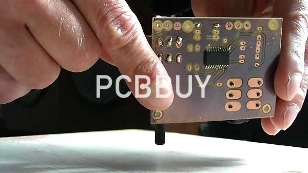
Accurate PCBs are essential for the optimal performance of devices. Checking your quality PCB design is as essential as the design itself. The PCBs hold the ICs and other components and implement the interconnections between them. PCBs are created in abundance for portable electronics, computers, and entertainment equipment. They are also made for test equipment, manufacturing, and spacecraft.
How to design high-quality PCB? If you are curious about the topic, please check and read the content below for more professional knowledge below.
What are the 5 tips of high-quality PCB design?
1. Inspect Traces in your PCB Design
Traces are wire conductors responsible for current flow from one component to another. In your PCB- the solder masks cover up the particles. A good practice to reduce errors is color-coding the masks. Traces of only the top and bottom layers of your PCB designs are visible. The usual solder mask color is green- although other colors are also available. White is difficult to notice.
Errors due to Trace misplacement are common. The usual golden rule is- Keep the trace connections as clean as possible. Traces with sharp bends can be problematic for higher power or frequency transmission. Try to avoid steep 90-degree angles. There are exceptions to this general rule too. PCBs with square concentric spirals are a perfect example. We can find these characteristics of high-quality PCB.
2. Pay attention to the schematic details
Schematics control the project, so accuracy and completeness are critical for success. They include information that is necessary for the proper operation of the circuit. A schematic should include adequate design details, such as pin numbers, names, component values, and ratings.

Embedded within each schematic symbol is the manufacturer part number used to determine price and specifications. The package specification determines the size of the footprint for each component. The first step should be to make sure the exposed copper for each pin is in the proper location and is slightly larger than the component pins (3 to 20 mils) depending on available area and soldering method.
3. To process the component placement
Component placement is next in the process and determined based on thermal management, function, and electrical noise considerations. A first-pass component placement step commences after the outline of component and interconnect position has been assigned. Immediately after the individual components are placed, a placement review should be held and adjustments made to facilitate routing and optimize performance.
Placement and package sizes are often reconsidered and changes are made at this point based on size and cost. Components absorbing greater than 10 mW or conducting more than 10 mA should be considered powerful enough for additional thermal and electrical considerations. Sensitive signals should be shielded from noise sources with planes and be kept impedance-controlled.
4. Follow the PCB trace length standards
Analyze the length of your PCB traces. For time-specific functions dependent on many signals- this is critical. High-speed clock signals, data, and address bus lines use these relative PCB functions. The bus lines connect the microprocessor with RAM. When checking the PCB quality, we should pay attention to:
The length matching ensures signal transmission through the same delay period. The signals arrive at the same time- passing through delay lines. Knowledge of the PCB layout and schematics is essential. Learn which signal line needs delay lines- and by how much.

Traces of only the top and bottom layers of your PCB designs are visible. The usual solder mask color is green- although other colors are also available. White is difficult to notice. Errors due to Trace misplacement are common. The usual golden rule is- Keep the trace connections as clean as possible. Traces with sharp bends can be problematic for higher power or frequency transmission.
5. Deal with the decoupling capacitors
All chips need power to function, but what happens when the power source is some distance away from the chip needing the power? In these cases, power has to be brought to the chip via a PCB trace (although typically via a PCB power plane on an inner layer).
Decoupling capacitors are placed very close to the chip’s power pins in order to filter out any high-frequency noise from impacting the chip negatively. In general, if a chip has more than one VDD pin, then each such pin requires at least one decoupling capacitor, sometimes more.
These decoupling capacitors should be physically placed very close to the pins they are supposed to decouple. If this doesn’t happen, their effect is greatly reduced. If your PCB design doesn’t have decoupling capacitors placed right next to the power pins on most of the microchips, then that is a big indicator that your design was not done properly.
Industry Category


