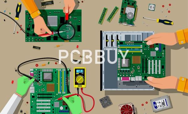
5 Tips of PCB Component Placement Guidelines for PCB Design
By:PCBBUY 09/22/2021 09:36

Today, the best placement of components on a board is not only the result of strict theoretical rules of electronics and it is greatly facilitated and aided by a powerful software that supports designers in the creation of very sophisticated electronic circuits.
And during the PCB design process, there are many useful tips to guarantee the quality and performance of the finished board. If you are going to learn more information about the PCB component placement, you can check and read the content below for more professional knowledge.
What are the 5 tips for PCB component placement?
1. Prepare factors for the PCB component placement
The primary objective of PCB development is to design a PCB that functions and performs as intended. However, it is equally, if not more, important for a design to be manufacturable. Of course, various determining factors may affect PCB manufacturability, including:
· Components: If a component is distinctive or challenging to acquire, it will increase the cost of manufacturing. Moreover, if the lead times on some components incur delays in production, it will increase costs.
· Placement: Component placement affects how you manufacture a PCB and whether you can even manufacture a PCB. Improper component placement can dramatically increase board costs. In fact, design decisions as simple as the orientation of a component can affect its solderability.
· Layout: The schematic layout places component placement and other considerations at the center of your design process. However, failure to account for possible connections or interfaces with other PCBs will increase overall system manufacturing costs.
2. Knowing the importance of component placement in PCB design
You won’t have to deal with your mom’s nagging when you place components on PCB according to your whims and fancies. But be prepared to face a barrage of complaints from unhappy clients or technicians when problems crept up in the field.

Improper component placement can lead to a horde of issues that affect functionality, durability, manufacturability, and serviceability of the PCB. For example, placing analog and digital components without proper segregation is a perfect recipe for the analog signal to be compromised.
3. Pay attention to the defects during PCB component placement
The majority of component placement problems that affect manufacturing are when components are placed too close to the edge of the board. This potentially can result in damage to the board from different sources, such as automated assembly equipment during a volume manufacturing run. Given below are some other placement considerations that you should keep in mind:
Place your fixed parts first. These parts include anything that has to interface with the rest of the system that your board is going to be used in for example Connectors, switches, etc. Mechanical parts such as nuts and bolts will also need to be placed in fixed locations. Before placing a part down, you should also know exactly where your mounting holes and edge connectors should go and what kind of mechanical enclosure to fit your board.

Components placed too close together could cause problems for automated pick-and-place machines during assembly and for testing. Keep at least 50mil space between components and 100mil space from component to board edge. Place connectors on one edge or on one corner of the board. Try to place all components on the top side of the PCB. If not possible, only place small size and low thermal dissipation components (like SMD passive parts) can be on the bottom side.
4. Process the best practices for PCB component placement
Although the design process may vary from design to design, designers follow some best practices for component placement. Some of them are:
· Orienting all similar components in the same direction for easier diagnosis and traceability. For instance, placing all polarized diodes, capacitors, LEDs with their cathodes either to the +X or +Y direction. Placing such information on silk screens or in the copper layer is helpful to manual assembly, reducing human error.
· Placing all Surface Mount Type (SMT) and Through Hole (TH) components on the same side of the board. This reduces the number of assembly steps.
· Following the Design for Manufacturing (DFM) guidelines of their organization. Proper structure of traces and pads can prevent skewed or tombstoned components.

5. Pay attention to the considerations about PCB component placement
The majority of component placement problems that affect manufacturing are when components are placed too close to the edge of the board. This potentially can result in damage to the board from different sources, such as automated assembly equipment during a volume manufacturing run. Here are some other placement considerations that you should keep in mind:
· Component spacing: Components placed too close together could cause problems for automated pick-and-place machines during assembly and for the fixtures used for testing.
· Missing solder mask between pads: This can lead to solder bridging during assembly, which can cause electrical shorts between pins.
· Incorrect surface mount pad sizes: When discreet SMT pad sizes are not the correct shape or are imbalanced due to differing trace sizes, one pad could reflow faster than the other. This can cause the part to lift up on one end in an effect called “tombstoning.”
· Component orientation and location for wave soldering: Discrete components should be placed so that both pins enter the solder simultaneously when the board goes through the wave. Larger parts should also not precede smaller parts to avoid shadowing, which could cause insufficient solder joints between component pins and their metal pads on the board.
Industry Category


