5 Tips of PCB Minimum Etch Technique for Best PCB Design Practices
By:PCBBUY 09/29/2021 09:11

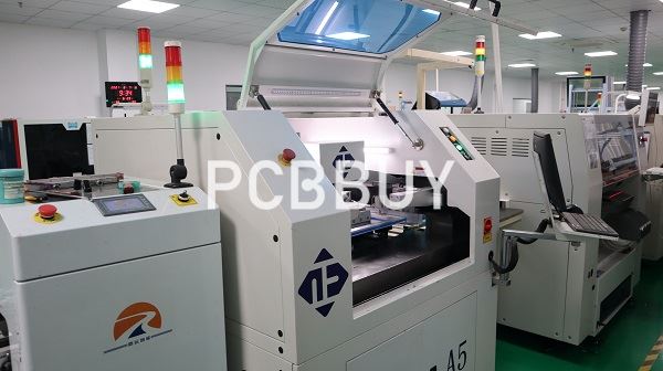
The process of PCB from light board to show circuit pattern is a more complex process of physical and chemical reaction. As etching is a very important finishing step of PCB manufacturing, we will analyze etching in this passage.
At present, the typical process of PCB is pattern plating etch process which means in the outer layer of the board to retain the copper foil part. That is, the graphic part of the circuit is pre-plated with a layer of tin lead corrosion layer. The remaining copper foil is then chemically etched away. The whole process is known as etching.
In this article, we will provide you PCB minimum etch techniques. If you are interested in the PCB etching, please check and read the content below for more information.
What are the main types of PCB etch?
What are the 5 tips of PCB minimum etch technique in design?
1. Getting to know the definition of PCB minimum etch
Even if you’ve never fabricated a PCB, you might be familiar with the process. PCB etching involves the application of UV-resistant laminate to a pre-sensitized photoresist copper layer, which is then exposed to UV rays. Areas that are not covered will be etched off in a special etching solution.
The PCB minimum etch technique has more to do with what happens at the design stage than the process of PCB etching itself. It refers to the idea of keeping as much copper area on the PCB as possible. Effectively, what minimum etch does is impose a tradeoff - it improves heat dissipation, while making parasitic capacitance more prominent.
2. The main types of PCB etching
Before the PCB etching, we should know the types of etching so that we could make out the difference of them. There are two layers of copper on the board when etched. In the outer layer of the etching process, only one layer of copper must be etched away, and the rest will form the final desired circuit.
Another method is the entire board is copper, photosensitive film outside the part is only tin or lead tin resist layer. This process is called “full board copper plating”. Compared with the graphics plating, the biggest drawback of the whole board copper plating is plated twice the copper surface and the etching must also be corroded them. So when the wire width is very fine will produce a series of problems.
3. Process the PCB wet etching
Wet etching is a technique in which etching materials are immersed in an etching solution for etching. It is the most common etching method. There are three factors that affect the etching rate of the etched object: etching solution concentration, etching solution temperature, and stirring. Qualitatively speaking, increasing the etching temperature and adding stirring can effectively increase the etching rate; The characteristic of wet etching is isotropic.

Advantages of wet etching
· Good surface uniformity.
· Good adaptability, suitable for almost all metals, glass, plastics, etc.
· Low cost.
· With excellent selectivity, the current film will stop after etching without damaging the film of other materials below.
4. Process the mechanical etching
In response to the inexorable tightening of environmental regulations and the difficulty of obtaining strong acids and oxidizers in many locales, "mechanical etching" has seen unprecedented growth over the last 10 years. In spite of high up-front costs and lack of plated through-holes, its complete freedom from toxic chemicals has made this technique very attractive to many PCB prototyping shops.
As the density and complexity of circuit designs have increased, forming reliable electrical connectivity between the top (component) and bottom (solder) circuit patterns has evolved from a mere convenience to an absolute necessity. While some mechanical etch vendors offer manual and semi-automatic machines for inserting eyelets into all of the designated through-holes, the cost of the equipment, the penalty in PCB real-estate, and the relative sluggishness of the process render it undesirable for many applications. As a result, many shops have adopted simplified electrolytic plating processes to accomplish this critical task.

5. Optimize the PCB minimum etch technique
There are bound to be uncovered areas on a PCB if you’re not taking proactive steps to optimize it with PCB minimum etch technique. Thankfully, it’s quite easy to ensure that you’re leaving as much copper area on the finished PCB as possible.
First, you’ll need to create a copper pour for the ground plane. Then, look for areas that are left out in the copper pour. Usually, these areas are not connected to the ground net. You’ll need to manually create a ground net in the area by using vias or by adjusting nearby traces to make space for a ground connection. Once that’s done, repour the ground plane.
By now, you ought to have a copper plane that’s covering most of the surfaces. There shouldn’t be any odd areas that are left uncovered. Finally, run a DRC check to ensure that all the segments of ground planes are connected.
Industry Category


