5 methods for through-hole treatment of PCB solder resist ink
By: 05/25/2023 17:20

According to the curing method, PCB solder resist ink can be classified into photosensitive ink, heat-curable ink, and UV-curable ink. Based on the type of board, there are PCB rigid board solder resist ink, FPC flexible board solder resist ink, and aluminum substrate solder resist ink. The solder resist ink for aluminum substrates can also be used on ceramic boards.
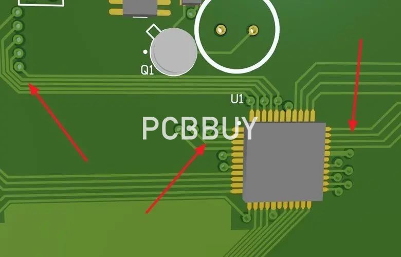
Through-holes are generally categorized into three types: blind vias, buried vias, and through vias. "Blind vias" are located on the top and bottom surfaces of the printed circuit board (PCB) and have a certain depth, used for connecting surface and inner layer circuits. "Buried vias" are internal connection holes in the PCB's inner layers and are not visible on the surface. "Through vias" penetrate the entire PCB, connecting the top layer to the inner layer and then to the bottom layer.
In the PCB solder resist process, common techniques for handling through-holes include via capping, via plugging, via tenting, resin filling, and conductive fill plating. Each of these techniques has its own characteristics.
If you want to order PCB product, please check and custom your order online.
NO.1: Via Capping
Via capping refers to covering the via pads with solder resist ink, without any solder on the pads. This technique is commonly used in most PCBs. It is recommended to avoid via diameters larger than 0.5mm, as larger diameters may result in ink quality issues inside the via. When converting PCB design files to Gerber artwork files, the via tenting feature should be disabled, as the via would appear as an open window instead of being capped.
NO.2: Via Tenting
Via tenting refers to leaving the via pads exposed with copper, which are then surface-treated with gold or tin. The purpose of via tenting is to allow the solder to flow into the via during wave soldering, increasing the via's current-carrying capacity. Via tenting has the same effect as through-hole plugging, and it doesn't require disabling the via tenting feature when converting to Gerber files.
NO.3: Via Plugging
Via plugging involves filling the via hole walls with solder resist ink. During production, solder resist ink is inserted into the vias using aluminum foil, followed by applying solder resist ink to the entire board. The purpose of via plugging is to prevent solder from flowing through the via during wave soldering and causing short circuits on the component side. When converting design files to Gerber files, the via tenting feature should be disabled.
NO.4: Resin Filling
Resin filling refers to filling the via hole walls with resin and then leveling the solder pads. This technique is suitable for any type of one-sided or two-sided windowed vias. The purpose of resin filling, from a process perspective, is to prevent the PP adhesive used during lamination from flowing into the hole if it is not resin-filled before lamination, which could lead to delamination and board failure. From a design perspective, if there are vias drilled on the solder pads, not filling them with resin before leveling would result in a smaller soldering area and poor soldering quality.
NO.5: Copper Fill Plating
Copper fill plating involves filling the via hole walls with copper and then leveling the solder pads. This technique is suitable for any type of one-sided or two-sided windowed vias. The purpose of copper fill plating is to accommodate high currents in large vias. The cost of copper fill plating is much higher than resin filling. When designing files, simply disable the via tenting feature.
Industry Category


