7 Essential Elements to Understanding PCB Schematics
By:PCBBUY 02/25/2022 10:44

Once you are working in your schematic capture system, there are some things that you can do to make sure that the design that you are creating will result in an easily assembled board: In this passage, you will get everything you want of PCB schematics. Please check and read the passage for more information.

What are the guidelines to draw a PCB schematic diagram?
To achieve a successful design, follow these standard schematic guidelines.
Page size selection
Most of the design tools offer different page sizes. Generally, the tools would select the page size as A4. However, it should be noted that various other page sizes are also available. Designers should select the size based on the size of their circuit design.
Page naming convention
The logical blocks of the schematic should be separated by pages. The pages can be named using the letters A, B, C, and so on. By doing this, we can place the pages in alphabetical order. An example of such a naming convention is shown below.
· Block Diagram
· Power supply
· MCU interface
· Memory interface
· Revision history
Block diagrams and revision history are often ignored by most designers to save time. However, they can be very helpful for other designers trying to understand the schematic. Most of the product-based organizations mandate all such protocols and regulations.
Grid setting
Though it is not a direct requirement of the designer, the tool needs to have some references. Hence the grid system is followed. Having grids helps the designer to reference the parts properly and make their connection. Circuit components and connections must always be on the grid, this helps in probing the nets during analysis.
What are differences between PCB schematics vs. PCB designs?
A PCB schematic is a simple two-dimensional circuit design showing the functionality and connectivity between different components. PCB designs, on the other hand, are three-dimensional layouts that indicate those components’ locations once you know your circuit works.
The PCB schematic, then, is the first part of designing a printed circuit board. It’s a pictorial representation, either written or on a computer, that utilizes agreed-upon symbols to describe circuit connections. It also indicates the components that will be used and how they are connected. Anyone should be able to pick up and read the PCB schematic.

Its name aptly describes it: the PCB schematic is a plan, a blueprint. Its concern is not where specifically the components will be located. Instead, the schematic lays out how the PCB will ultimately achieve connectivity and forms a critical part of the planning process.
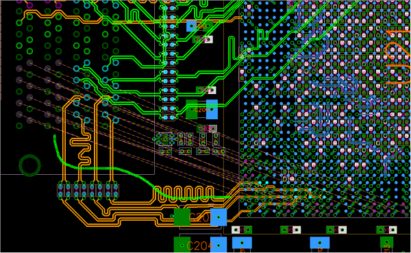
Once the blueprint has been completed, the PCB design comes next. The design is the layout, or physical representation of the PCB schematic and includes the copper track and hole layout. The PCB design does show the locations of the components mentioned above, as well as their connections with copper.
PCB design is the phase that’s concerned with performance. Engineers build the real components on top of the PCB design, allowing them to test whether the device works or not. We mentioned before that anyone should be able to understand a PCB schematic, but the functionality is not readily understood by looking at the prototype.
The Basic Schematic
A schematic consists primarily of components and wires connected in such a way as to produce the desired electrical behavior. The wires will become traces or copper pours.

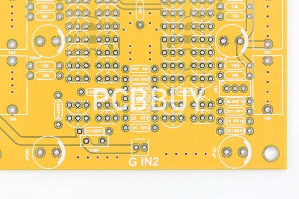
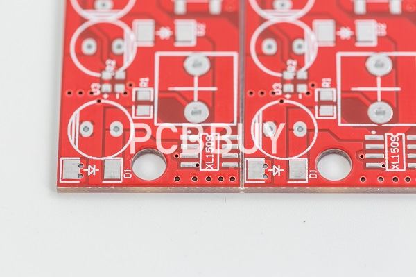
The components include a footprint (AKA land pattern), i.e., a collection of through-holes and/or surface-mount pads that match the terminal geometry of the physical part. A footprint can also have lines, shapes, and text that are collectively referred to as the silkscreen. These show up on the PCB as purely visual elements; they’re not conductive and do not affect the functionality of the circuit.
The Basic Schematic
A schematic consists primarily of components and wires connected in such a way as to produce the desired electrical behavior. The wires will become traces or copper pours.
The components include a footprint (AKA land pattern), i.e., a collection of through-holes and/or surface-mount pads that match the terminal geometry of the physical part. A footprint can also have lines, shapes, and text that are collectively referred to as the silkscreen. These show up on the PCB as purely visual elements; they’re not conductive and do not affect the functionality of the circuit.
Industry Category


