7 Essential Tips of PCB Heat Dissipation Techniques
By:PCBBUY 10/13/2021 10:19

Thermal modeling is a critical tool that is used to conduct thermal failure analysis. It gives designers a good understanding of various thermal issues associated with their circuit design. Also, it helps in choosing proper cooling methods and PCB design techniques.
PCB designers can figure out the optimum d esign and positioning of different components in the layout using suitable modeling software. Thermal modeling enables the designer to efficiently figure out the following aspects- heat flow pattern, heat sink design, and cooling methods for active devices. If you are looking for more information for PCB heat dissipation techniques, please check and read the content below.
1. Why is PCB heat dissipation techniques important?
Each working component will act as a heat source, and it is unavoidable that the temperature of your board will increase during operation. As a result, you need to have a strategy to remove heat from active components and spread it throughout your circuit board in order to keep your component temperatures within acceptable limits.
Thermal design and simulation software can help you validate your thermal strategy during design time. This requires some knowledge of the thermal properties of your circuit board substrate material and your components.
2. What are the special techniques of PCB heat dissipation?
Passive heat techniques are the easiest to implement, both from component selection, PCB layout, PCB material selection, and stackup design perspectives.
Learn more about passive thermal management techniques for your circuit board.
· Devices that run at high current will require some particular thermal management strategies that can also be used in board with lower current. Learn more about thermal management for high current circuit boards.
· Thermal design, power integrity, and signal integrity in a circuit board are all intimately related. You can use a simulation-driven workflow to validate your thermal design strategy and ensure that your circuit board temperature stays within acceptable limits.
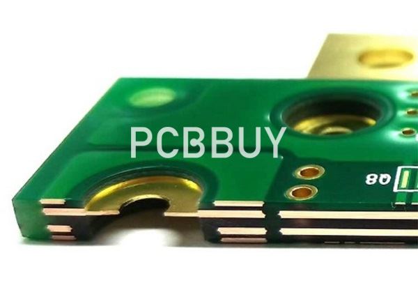
3. Pay attention to thermal via arrays
You can turn a PCB into an onboard heat sink by incorporating thermal via arrays over copper-filled areas, as shown above. The idea behind doing so is to have heat flowing from components to the copper area and dissipating through the air from the vias. Usually, thermal via arrays are used for power management modules and components with thermal pads.

When implementing thermal via arrays, remember that it needs to have a reasonably large diameter, in the region of 0.1 mm, for the heat to be dissipated effectively. Also, ensure the vias are not thermal-relief pads but padded holes that are connected to the copper area at all sides. Increasing the number of thermal vias further helps with heat dissipation.
4. How to reduce heat resistant?
A low thermal resistance ensures that the heat is transferred through the material much faster. This resistance is directly proportional to the length of the thermal path and inversely proportional to the cross-sectional area and thermal conductivity of the thermal path.
Thermal resistance \[\theta = \frac {t}{A \times K}\]
Where
· t is the thickness of the material
· K is the thermal conductivity factor
· A is the cross-sectional area
5. How to choose the right material for PCB heat dissipation?
There are materials other than epoxy resins that are better suited to dissipate disproportionate levels of heat such as polyimides or metal cores. If these materials are used, the decision has to be made upfront as these materials will have very different electrical characteristics, completely changing the structure of the design.
6. How to process routing for PCB heat dissipation?
The more metal that is on the board, the more the heat can dissipate through it. At the same time, power components require short routes to keep their inductance low. To satisfy both needs, use wider traces and/or more copper weight. For ground nets, it is best to use solid metal planes whenever possible as long as you can maintain the short and direct routing requirements.
7. How to balance the layout for effective PCB heat dissipation?
A number of PCB design techniques can be used to control the distribution of heat without additional cost. Here are some tips to bear in mind for your next design:

Temperature-sensitive devices are best placed in the lowest temperature regions (such as the bottom of the device). Never place it directly above the heating device. It is best to stagger multiple devices on the horizontal plane.
Heat sources on the same printed board should be arranged as far as possible to each other according to the degree of heat output. Low heat generating components or parts with low thermal resistance (such as small signal transistors, small integrated circuits, electrolytic capacitors, etc.) can be placed upstream to the cooling fan, while high heat generating devices or devices with high thermal resistance (such as power transistors, large scale integrated circuits, etc.) should be placed downstream of the cooling flow.
The device with the highest power consumption and heat output should be placed where heat dissipation is the most optimal. Do not place high heating devices at corners and edges of the printed board unless there is a heat sink nearby. When designing the power resistor, choose a larger device as much as possible, and allow enough space for heat dissipation when adjusting the layout of the printed board.
Industry Category


