Phone:+86 18806715434

Service Time:China:9:00 - 18:00

China Time Zone(GMT+8)(Update in 5 mins)

Cart ()

7 Main Aspects of Gold Finger PCB Specification in Manufacturing Process

By:PCBBUY 08/01/2022 14:37
7 Main Aspects of Gold Finger PCB Specification in Manufacturing Process

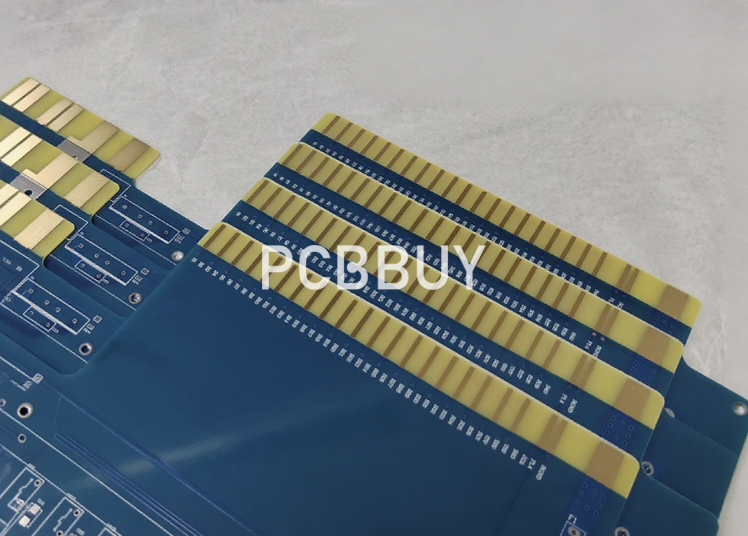
The process of PCB gold finger beveling is unavoidable in terms of making insertions quicker and more effortless. Unless the gold finger beveling is completed, insertions will be more difficult than usual. If you are going to learn more knowledge of gold finger PCB, please check and read the content below.

PCB Instant Quote


How Gold Fingers Are Applied

Gold fingers have multiple uses based on design:


  • Transfer network data.

  • Connect external components to PCB prototypes.

  • Attach adapters or daughter boards.

  • Act as audio adapters.

Use in PCBs

Gold fingers connect adjoining PCBs, with gold protecting edges from wear. They allow up to 1,000 connect/disconnect cycles.


  • Interconnection points: Facilitate signal conduction between peripherals/internal cards and computers via slots like PCI.

  • Special adapters: Enable PC performance boosts (e.g., better graphics/sound) via secondary PCBs.

  • External connections: Link peripherals (speakers, printers) to motherboards.

  • They also supply power to module PCBs, enabling device functionality and allowing computer upgrades over years.

Design Specifications

  • No copper on internal layers near PCB edges (to avoid exposure during chamfering).

  • Avoid PTH within 1mm of gold fingers.

  • Keep ≥0.5mm between gold fingers and PCB outline (compromising this causes failure).

  • No solder mask or screen printing near gold fingers.

  • Position gold fingers with PCB center facing outward.

IPC Standards

  • Chemical composition: 5–10% cobalt in gold plating for rigidity.

  • Thickness: 2–50 microinches.

  • Appearance test: Smooth, clean contact edges (no excess nickel) via magnifying glass.

  • Tape test: Check gold plating adhesion; gold on tape means inadequate coating.


gold fingers.png


What are the design specifications of gold fingers in PCB?


1. The internal PCB layer towards the edge of PCB must be free of copper to prevent exposure during chamfering.


2. It is not recommended to include PTH within 1mm of gold finger.


4. Keep a distance of at least 0.5mm between the gold finger and the circuit board outline.


5. Any compromise of the standard spacing values can lead to PCB weakness and failure.


6. Do not use anti welding or screen printing near the golden finger.


7. The gold finger shall be placed at the position with the PCB center facing outward.


The IPC has set some standards for the production of PCB gold fingers. IPC standards are summarized as follows:


Dimensions

x

Quantity

Layers

Quote Now

PCB Instant Quote

Dimensions

x mm

Quantity

Quote Now