7 PCB Test Points Rules to Improve Manufacturing Process
By:PCBBUY 09/27/2021 10:10

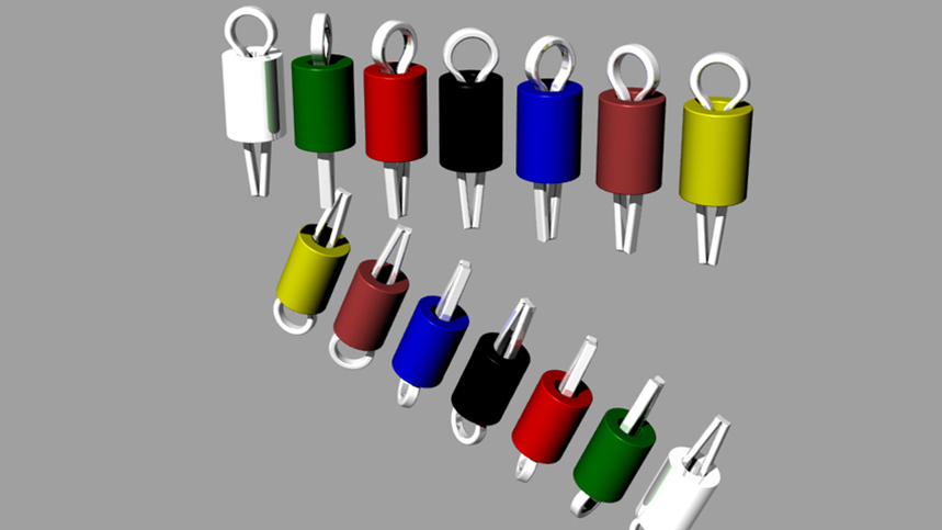
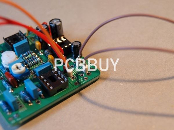
A PCB test point is a small wire loop used for test probes on a PCB that contains surface-mount parts. During production, they enable the user to inject test signals or monitor the board’s circuitry. Test points come in a variety of materials, sizes and colors.
In this article, we will tell you the test point rules to improve the PCB manufacturing. If you are interested in the PCB point rules, welcome to check and read the content below for more professional knowledge to learn it.

What are the main 7 rules of PCB test point?
1. The purpose of PCB test point
The purpose of setting test points is to test whether the components on the circuit board meet the specifications and solderability. For example, if you want to check the resistance of a circuit board, the simplest method is to measure it with a multimeter You can know both ends.
In the early days when traditional plug-in (DIP) was used on the circuit board, the solder pins of the parts were indeed used as test points. The misjudgment situation of poor contact occurs, because after the general electronic parts are subjected to wave soldering or SMT tin eating, a residual film of solder paste flux is usually formed on the surface of the solder, and the resistance of this film Very high, which often causes poor contact of the probes.
2. The types of PCB test point
There are three main test systems that will use these test points on the board:
Bare board test: This is a test that is run after the circuit board has been fabricated to make sure that all of the nets in the board have electrical connectivity.
In-circuit test: ICT is run after the board has been assembled. The board is positioned on the ICT fixture which is filled with probes for each individual net.
Flying probe: Like ICT, this test is run after assembly on each net of the board by accessing the test points.

3. The limitations of PCB test point
There are some inherent limitations in the use of needle beds for circuit testing, such as:
The minimum diameter of the probe has a certain limit, and a needle with a too small diameter is easily broken and damaged.
Needles cannot be implanted next to some high parts. If the probe is too close to the high part, there is a risk of damage to the high part. In addition, because the part is relatively high, it is usually necessary to open a hole in the test fixture needle bed seat to avoid the needle implantation.
The distance between the needles is also limited, because each needle must come out of a hole, and the rear end of each needle also needs to be welded with a cable. Test points for all parts that are increasingly difficult to accommodate on the circuit board.
4. The advantages of PCB test point
Low profile: Compared to other test probe connection types, test points offer a much lower profile. Alternatives such as posts and turrets may not fit in a thin enclosure. Test points have a profile similar to that of surface-mounted components, making them a more versatile choice.
Time and cost savings: By detecting connectivity issues through test points in early design phases, you can save time and money in later stages. Without early testing, a PCB can demonstrate issues in later design phases that involve more expensive assemblies.
Easier error detection: Test points simplify the probe testing process, making it easier to detect potential issues. With test points, you can get the measurements you need without compromising your PCB design.

5. Widely applications of PCB test point
The test points in the TP and ATP series lines are designed to satisfy a range of applications, including:
· Medical Devices
· Security Electronics
· Industrial Electronics
6. Hidden issues of PCB test point
Worse still are subtle problems that affect the products long term performance. Sensor accuracy and power consumption are two issues that could be caught at the populated PCB stage but which may find their way into a customer’s hands untested.
Finding faults early using test points makes it cheaper and saves on cost and quality issues. It also gives you something you can’t measure. Peace of mind. Often at the production stage it can be tempting to assume that testing processes are robust but using a test fixture takes this to the next level of certainty.
7. The process to create PCB test point
To function as a PCB test point, the test point must be an exposed metal spot on an exterior layer of the board that is connected to a net. This will allow the probes of the automated test equipment to make contact with it to conduct the test.
The next step is to flag the desired locations as test points in the CAD system. The design software typically will then go through and automatically select test point candidates if they conform to spacing and other specific requirements set up in the parameters.
Once each candidate has been flagged as a test point, the PCB design software is ready to export this information into a test point file.
Industry Category


