7 Tips of PCB Footprint Design Guidelines for Beginners
By:PCBBUY 09/29/2021 09:37

Just like your PCB design, your component footprints must also always adhere to certain restrictions. Therefore, every board design should institute footprint pad layout guidelines. Before defining the best footprint pad layout guidelines to follow, let’s first take a look at what footprint pad layout guidelines are; why they’re important, especially for your design for assembly (DFA); when you need to use them; and how to do so.
In this article, we will provide you all the details about PCB footprint design. If you are going to learn more knowledge about PCB footprint design, please check and read the content below for more information.

What are the 7 tips of PCB footprint design for beginners?
1. Learn the importance of PCB footprint design
Components are the most important elements of the board, and pads are the points of connection. If the pad layout fails to accurately identify your component locations or isn’t arranged such that the component can be securely attached, the PCB cannot be assembled. If the pads don’t line up properly with other surface elements like traces and drill holes, your board will not function properly or at all. Just like your PCB layout, your component footprints must also always adhere to certain restrictions. Therefore, every board design should institute footprint pad layout guidelines.
2. Get into know PCB component footprint design knowledge
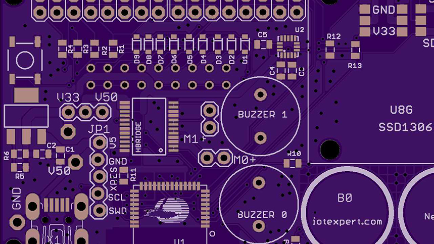
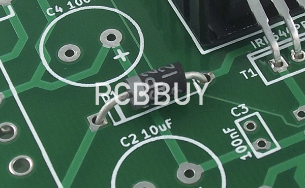
Your PCB component footprints should include several basic pieces of information. Things like placement, assembly, and silkscreen outlines, reference designators and part numbers are all invaluable and should be present in a component footprint. Your CAD tools are invaluable here as you can create your 2D footprints in a variety of file formats. However, it is best to use the CAD tools in your PCB design software to ensure file compatibility. There are four important points to remember when creating PCB footprints:
· Keep Your Datasheets Handy
· Watch for SMD Pad/Through-hole Locations and Sizes
· Understand Standard Package Sizes
· Include Polarity and Pin-1 Indicators
3. Start with PCB footprint creation
There are several ways to create your PCB footprint library, and the first is to use existing library parts. In many cases, the vendor or supplier of the PCB design tools you are using will already have vast libraries from which you can pull parts. There are also many component vendors out there who will offer a footprint of the specific part you are using tailored for the design tools that you are working on. The advantage here is that, since these footprints are created by the component vendor, they are usually very accurate.

4. Pay attention to issues during PCB footprint
When PCB design tools first became commonplace, there often wasn’t enough attention put into the creation of their library parts. Since design technology was less advanced and tolerances were more forgiving in those days, designers were able to get by following less-strict guidelines
Incorrect pad sizes: Pads that are too small can cause breakout problems for through-hole parts and bad solder joints for surface mount technology (SMT) parts.
Pads that are not spaced correctly: Through-hole pads that are too close together or too far apart can cause problems with component insertion during assembly.
Component outlines that are too small: Footprints that have their body outlines drawn too small will not be able to be assembled using automated production lines.
5. Get into the considerations PCB footprint
This shows where mounting pads (for SMD components) or mounting holes (through-hole components) are located. These locations are used for soldering and must be designed accurately. This act like a keepout area in your PCB footprint, i.e., other components cannot be placed within the PCB footprint courtyard.

6. The methods to create PCB footprint
The footprint or land pattern is an arrangement of plated copper pads or through-hole plated pads on a PCB on which a component is soldered. Most of the time, the board footprints of standard packages are available in the PCB library of the design software. Only if it is not available, we will have to create one on our own referring to the datasheet of the component, while designing a circuit board.
The created circuit board footprint should always match the component physical dimensions or else it will not align properly with the pads. The land pattern gives information regarding the pad sizes, the distance between the pads (pitch), component boundary and keep-out, silkscreen outlines, part numbers, reference designators, and pin numbering.
7. The standards for PCB footprint
IPC-7351 is one of the many standards developed and published by IPC Association Connecting Electronics Industries. Since its founding in 1957, IPC has been at the forefront of standardization for the design, manufacturing and testing of PCBs and PCBAs.
· Use a common package type, if possible, as a starting point for your design
· Follow IPC standard dimension and tolerance guidelines
· Incorporate testability into your design
· Ensure that standard specs adhere to your CM’s DFM
· Allow access space for rework
Industry Category


