PCB Layout Guidelines: 7 Tips of PCB Grounding Techniques
By:PCBBUY 09/23/2021 09:17

A ground is a conducting body that acts as an arbitrary node of potential voltage and a common return for electric current. It is a point of zero reference or zero volts. The ground is the reference against which you base the signal. In a circuit with one battery with a positive and negative terminal, the negative terminal is usually called the ground.
Grounding is a critical concept for any electronic circuit and any system dealing with an electric current. Everything from the electric grid to a home to a printed circuit board has a ground. PCBs are critical to the functioning of nearly all electronics, and each PCB needs proper grounding to function correctly.
In this passage, we will tell you everything about the tips of PCB grounding techniques. If you are interested in the PCB grounding techniques, please check and read the content for more information.

What are the 7 tips of PCB grounding techniques?
1. Different types of PCB grounding techniques
Following are the different types of nodes that are referred to as grounds-
· Floating grounds: A floating ground is simply a large reference conductor in an isolated system. A floating ground is not physically connected to earth.
· Earth ground: This is literally a physical connection to the earth. This acts as a safe return point to deplete surplus current.
· Chassis ground: The electronics in a PCB cannot connect directly to an earth ground (this normally happens through the power supply), but the metal chassis can act as a good ground. This is usually used to ground the body of an enclosure as a safety measure.
· AC ground: These are low impedance ground paths that block DC return current. This is normally created by connecting to a ground plane through a capacitor.
· Virtual ground: These grounds can be found in negative feedback circuits at the inverting end of operational amplifiers. Connecting 0 V to the non-inverting input will pull the inverting input 0 V, and this value is usually held constant through feedback. This is an unstable node and cannot be used as a return path for other circuits.

2. Different areas of PCB grounding techniques
Grounding techniques can be generally divided into two areas:
· Placing power and ground planes in your layer stack.
· Arranging components in order to provide short, reliable return paths to ground.
3. Ensure the proper PCB grounding techniques
Generally, if you place components on the surface layer, you’ll want to place components on the signal layer directly above the ground layer. This allows you to route return signals directly to ground and ensures that traces remain tightly coupled to your ground layer. Placing components and signals directly above the ground layer also minimizes the loop area, which reduces susceptibility to EMI.
Some PCB designers recommend that you use two different ground planes on the same layer: one for digital components/signals, and the other for analog components/signals. They will then tell you to connect the two ground planes with a ferrite bead or a capacitor.
4. Pay attention to ground plane
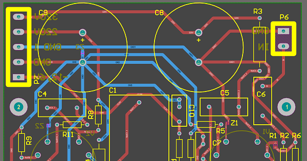
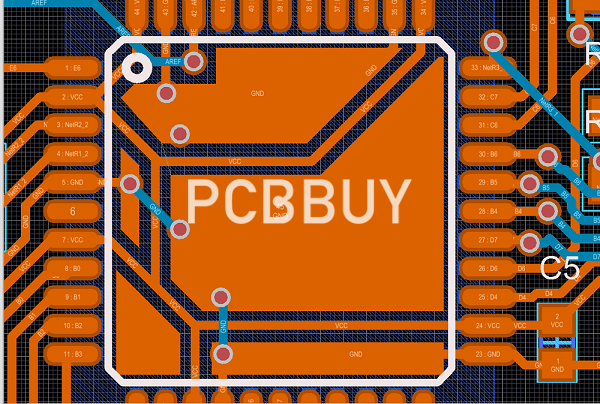
A ground plane is a piece of copper on the board covering a large area. It is a good practice to cover all places on the board that do not contain a component or a trace with the ground plane. A trace is a thin piece of copper on the board that connects two components together. It acts like a copper wire. Generally the ground plane is made on both sides of the board, but the component side plane is sometimes kept at the supply voltage while the plane on the other side is grounded. The ground plane should be connected to all the ground pins of components and connectors. This helps keep the ground voltage at the same level throughout the board.
5. Getting to know the grounding strategy
One of the first decisions will be deciding what the grounding strategy will be. Lower frequency applications will sometimes use a single point or “star” grounding technique, where the different grounds are tied together only at one point on the board. Higher frequency boards will use a multi-ground strategy where all ground connections on the board share the same plane through low impedance connections. The shortened connections of this technique help to reduce the EMI that can be created at higher frequencies.

6. Process the ground plane vias
Two ground planes are added on both sides of the PCB and are interconnected using vias at different places of the board. They are holes that connect each side and allows to access the ground plane from anywhere.
The vias mainly connect the components directly through low impedance to all of the circuit’s other ground points. The common practice adopted is most scenarios is placing ground vias at one-eighth of a wavelength. This is because a stub on a trace only starts to become an issue at one-eighth of a wavelength.
7. Pay attention to decoupling
PCBs contain one or more integrated circuit chips, which require power to operate. These chips have supply pins to connect them to an external power source. They also have ground pins, which connect them to the ground plane of the PCB. Between the supply and ground pins, there is a decoupling capacitor, which serves to smooth out oscillations in the voltage being supplied to the chip. The opposite end of the decoupling capacitor connects to the ground plane.
One of the main reasons for the use of decoupling capacitors is related to functionality. A decoupling capacitor can act as a charge storage device. When the integrated circuit (IC) requires additional current, the decoupling capacitor can provide it through a low inductance path. Because of this, it is best to place decoupling capacitors close to the IC power pins.
Industry Category


