
AI Server PCB Stackup Design Guidelines: Layer Structure
By:PCBBUY 07/30/2026 17:08
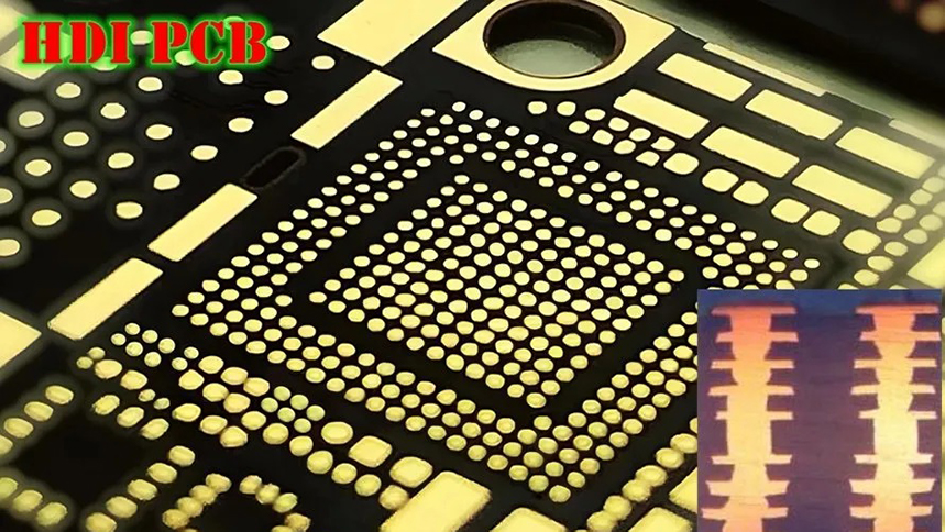
The rapid growth of artificial intelligence, machine learning, and high-performance computing has significantly increased the requirements for server hardware. Modern AI servers integrate powerful GPUs, CPUs, memory modules, high-speed interconnects, and advanced power delivery systems, creating extremely demanding PCB design challenges.
Unlike conventional server boards, AI server PCBs must handle:
-
Ultra-high-speed data transmission
-
High power density
-
Complex power distribution networks (PDN)
-
Advanced thermal management
-
High layer count routing requirements
A well-designed PCB stackup is essential to maintain signal integrity, power integrity, thermal reliability, and manufacturing consistency.
Understanding AI server PCB stackup design guidelines helps engineers optimize layer structures, select suitable materials, control impedance, and improve overall system reliability.
As a professional PCB manufacturer, PCBBUY provides high-layer-count PCB fabrication,
HDI technology, controlled impedance manufacturing, high-speed material processing, and advanced inspection capabilities to support next-generation AI server applications.
What Is an AI Server PCB Stackup?
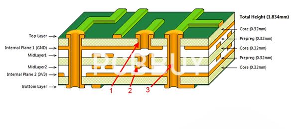
A PCB stackup defines the arrangement of copper layers, dielectric materials, power planes, and signal layers within a multilayer PCB.
For AI server applications, the stackup design determines:
-
Signal transmission quality
-
Power delivery performance
-
Heat dissipation capability
-
Electromagnetic interference (EMI)control
-
Manufacturing reliability
A typical AI server PCB may contain:
-
Signal layers for high-speed routing
-
Ground planes for signal return paths
-
Power planes for GPU/CPU power delivery
-
Low-loss dielectric layers
-
Multiple reference layers for impedance control
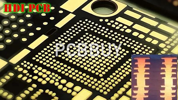
Why AI Server PCB Stackup Design Is More Challenging?
AI servers require significantly higher performance compared with traditional computing platforms.
|
Challenge |
Impact on PCB Design |
|
High-Speed Interfaces |
Requires strict impedance control |
|
Large GPU Power Demand |
Requires heavy copper and robust power planes |
|
High Component Density |
Requires HDI and fine-line routing |
|
Thermal Load |
Requires stable materials and thermal management |
|
EMI Requirements |
Requires optimized layer arrangement |
Key AI Server PCB Stackup Design Guidelines
1. Use Dedicated Signal and Reference Plane Structures
High-speed signals require a continuous reference plane to minimize return path disruption.
A common principle is:
Signal Layer → Ground Plane → Power Plane → Signal Layer
This structure helps:
-
Reduce electromagnetic interference
-
Improve signal integrity
-
Control impedance
-
Reduce crosstalk
Example High-Speed Layer Arrangement
|
Layer |
Function |
|
L1 |
Component / High-speed signal routing |
|
L2 |
Ground reference plane |
|
L3 |
High-speed signal layer |
|
L4 |
Power distribution |
|
L5-L6 |
Memory and interface routing |
|
Inner Layers |
Power and ground planes |
|
Bottom Layers |
Signal routing and components |
2. Select Low-Loss Materials for High-Speed AI Server PCBs
AI servers commonly support interfaces such as:
-
PCIe Gen5/Gen6
-
112G Ethernet
-
High-speed SerDes
-
DDR5 memory
These systems require low-loss PCB materials.
Important material parameters include:
|
Material Parameter |
Importance |
|
Low Dissipation Factor (Df) |
Reduces signal loss |
|
Stable Dielectric Constant (Dk) |
Maintains impedance accuracy |
|
Low CTE |
Improves thermal reliability |
|
Low Moisture Absorption |
Prevents electrical variation |
|
High Tg |
Improves heat resistance |
PCBBUY supports:
-
High-TG FR-4 materials
-
Rogers high-frequency laminates
-
Low-loss materials
-
Hybrid material stackups
3. Optimize Impedance Control for High-Speed Interfaces
AI server PCBs require precise impedance matching to prevent:
-
Signal reflection
-
Data errors
-
Timing issues
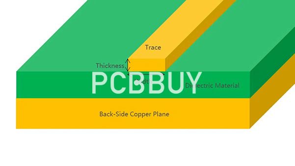
Typical controlled impedance structures include:
|
Structure |
Application |
|
Microstrip |
External high-speed signals |
|
Stripline |
Internal differential pairs |
|
Differential Pair Routing |
PCIe, Ethernet, memory interfaces |
Common AI Server Signal Requirements
|
Interface |
Typical Design Requirement |
|
PCIe Gen5/Gen6 |
Differential impedance control |
|
DDR5 |
Tight timing matching |
|
112G Ethernet |
Ultra-low-loss transmission |
|
High-Speed SerDes |
Stable signal integrity |
PCBBUY provides controlled impedance PCB manufacturing with strict process monitoring.
4. Increase Layer Count for Complex AI Server Routing
AI server motherboards require extensive routing space due to:
-
Multiple GPUs
-
High-speed memory channels
-
Large power networks
-
High-density connectors
Compared with standard PCBs, AI server boards often require higher layer counts.
|
PCB Type |
Typical Layer Requirement |
|
Consumer Electronics |
2-8 layers |
|
Industrial Control |
4-12 layers |
|
Server PCB |
12-24 layers |
|
AI Server PCB |
16-30+ layers depending on design |
PCBBUY supports high multilayer PCB manufacturing from prototype to volume production.
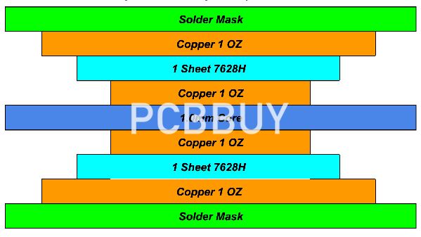
5. Design Effective Power Delivery Network (PDN)
AI processors require extremely stable power delivery.
The PCB stackup should include:
-
Dedicated power planes
-
Multiple ground layers
-
Short current return paths
-
Low impedance power structures
|
PDN Design Element |
Benefit |
|
Thick Copper Layers |
Handles higher current |
|
Multiple Power Planes |
Reduces voltage drop |
|
Closely Coupled Power/Ground Layers |
Improves power integrity |
|
Low-Loss Dielectrics |
Reduces power noise |
PCBBUY supports customized copper thickness solutions for high-current PCB applications.
6. Consider Thermal Management in Stackup Design
AI servers generate significant heat from:
-
GPUs
-
CPUs
-
Accelerators
-
Voltage regulator modules (VRMs)
PCB stackup design should consider:
|
Thermal Solution |
Purpose |
|
Heavy Copper Layers |
Improve heat spreading |
|
Thermal Vias |
Transfer heat between layers |
|
High-TG Materials |
Maintain stability at high temperatures |
|
Copper Balance |
Reduce warpage |
AI Server PCB Stackup Material Comparison
|
Material Type |
Signal Performance |
Thermal Performance |
Application |
|
Standard FR-4 |
Medium |
Good |
General servers |
|
High-TG FR-4 |
Good |
Better |
Industrial servers |
|
Low-Loss FR-4 |
Excellent |
Good |
High-speed computing |
|
Rogers Materials |
Excellent |
Excellent |
Advanced AI/network systems |
|
Hybrid Stackup |
Optimized |
Optimized |
High-performance servers |
HDI Technology in AI Server PCB Stackup Design
As AI systems become more compact, HDI technology helps solve routing challenges.
HDI advantages include:
|
HDI Feature |
Benefit |
|
Laser Microvias |
Higher routing density |
|
Stacked Vias |
Better space utilization |
|
Blind Vias |
Improved signal performance |
|
Via Filling |
Enhanced reliability |
PCBBUY provides HDI PCB manufacturing capabilities including:
-
Laser drilling
-
Sequential lamination
-
Microvia processing
-
Stacked via structures
Manufacturing Considerations for AI Server PCB Stackup
A theoretically optimized stackup must also be manufacturable.
Important manufacturing factors include:
|
Manufacturing Factor |
Importance |
|
Layer Registration |
Prevents alignment errors |
|
Copper Thickness Control |
Maintains electrical performance |
|
Lamination Control |
Prevents delamination |
|
Material Compatibility |
Ensures reliability |
|
Impedance Verification |
Confirms signal performance |
PCBBUY manufacturing capabilities include:
|
Capability |
Specification |
|
Layer Count |
4-26 layers |
|
Minimum Line Width |
35μm / 1.4mil |
|
Minimum Hole Size |
0.1mm |
|
Registration Accuracy |
±25μm |
|
Alignment Control |
±12μm |
|
Maximum Copper Thickness |
Up to 10oz |
AI Server PCB Testing and Quality Assurance
High-performance server PCBs require comprehensive validation.
|
Testing Method |
Purpose |
|
TDR Testing |
Verify impedance |
|
AOI Inspection |
Detect circuit defects |
|
Flying Probe Testing |
Electrical verification |
|
Microsection Analysis |
Check internal structures |
|
Thermal Testing |
Evaluate reliability |
|
X-Ray Inspection |
Inspect hidden defects |
PCBBUY integrates multiple inspection procedures to ensure PCB consistency from prototype manufacturing to mass production.
PCBBUY Capabilities for AI Server PCB Manufacturing
For customers developing AI computing hardware, PCBBUY provides:
|
Capability |
Advantage |
|
High-Layer Multilayer PCB |
Supports complex AI server designs |
|
HDI Manufacturing |
Enables dense routing |
|
Low-Loss Material Processing |
Improves signal integrity |
|
Controlled Impedance Fabrication |
Supports high-speed interfaces |
|
Heavy Copper Capability |
Supports power delivery |
|
Advanced Testing System |
Ensures reliability |
Best Practices for AI Server PCB Stackup Design
|
Design Practice |
Benefit |
|
Place high-speed signals near reference planes |
Reduce noise |
|
Use low-loss materials |
Reduce transmission loss |
|
Maintain consistent dielectric thickness |
Improve impedance control |
|
Minimize via transitions |
Improve signal quality |
|
Balance copper distribution |
Reduce warpage |
|
Work with experienced PCB manufacturers |
Improve production yield |
Conclusion
As AI computing continues to push the boundaries of processing power and data transmission speed, PCB stackup design has become a critical factor in system performance.
Effective AI server PCB stackup design guidelines require careful consideration of:
-
Layer arrangement
-
Low-loss materials
-
Signal integrity
-
Power delivery
-
Thermal management
-
Manufacturing capability
By combining high-layer PCB fabrication, HDI technology, controlled impedance processing, advanced materials, and strict quality control, PCBBUY provides reliable PCB manufacturing solutions for AI servers, data centers, and next-generation computing platforms.
FAQ
1. Why is PCB stackup design important for AI servers?
AI servers require extremely high-speed data transmission and high power delivery. Proper stackup design improves signal integrity, power stability, thermal performance, and overall reliability.
2. How many layers does an AI server PCB typically require?
AI server PCBs often require 16 or more layers, depending on GPU quantity, memory channels, power requirements, and routing complexity.
3. What materials are recommended for AI server PCBs?
Common choices include:
-
Low-loss FR-4
-
High-TG laminates
-
Rogers high-frequency materials
-
Hybrid material structures
4. How does PCB stackup affect signal integrity?
Stackup determines:
-
Impedance control
-
Signal return paths
-
Crosstalk performance
-
Electromagnetic interference
A poor stackup can cause signal loss and communication errors.
5. Why are HDI technologies used in AI server PCBs?
HDI enables higher routing density, smaller via structures, and better support for high-pin-count processors and advanced components.
6. What testing is required for AI server PCBs?
Common tests include:
-
TDR impedance testing
-
Electrical testing
-
AOI inspection
-
Microsection analysis
-
Thermal reliability testing
7. Can PCBBUY manufacture AI server PCB stackups?
Yes. PCBBUY supports high-layer-count PCB manufacturing, HDI technology, controlled impedance fabrication, low-loss materials, heavy copper processing, and advanced quality inspection for demanding AI server applications.
Industry Category








