AOI Inspection PCB of Ensuring High-Quality Manufacturing
By:PCBBUY 08/20/2025 15:46

Introduction: What Is AOI Inspection PCB?
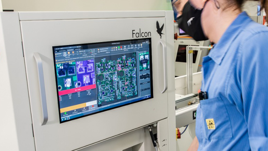
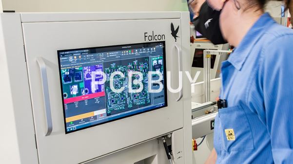
In the world of printed circuit board (PCB) manufacturing, quality control is a critical factor that determines the reliability of the final product. AOI inspection PCB (Automated Optical Inspection) refers to the process of using advanced optical systems and algorithms to automatically detect defects during PCB fabrication.
At PCBBUY, we integrate AOI inspection into every stage of production to ensure that each PCB meets the highest international quality standards. This process is especially important for high-density, multilayer, and precision PCBs used in industries such as automotive, medical, telecom, and consumer electronics.
Why AOI Inspection PCB Is Essential in Manufacturing
The AOI inspection PCB process plays a vital role in ensuring product consistency and reliability. Unlike manual inspection, which is time-consuming and error-prone, AOI offers several advantages:
-
Speed and Accuracy – High-speed cameras capture detailed images, allowing detection of even microscopic defects within seconds.
-
Comprehensive Coverage – AOI identifies defects such as:
-
Missing or incomplete pads
-
Open circuits and shorts
-
Solder paste misalignment
-
Broken or narrowed traces
-
Improved Yield – Early detection prevents defective boards from moving further down the production line, reducing scrap and rework.
At PCBBUY, we have implemented a multi-layer AOI inspection system, ensuring that both inner and outer layers undergo strict checks before final assembly.

How AOI Inspection PCB Works in Production
The AOI inspection PCB process involves several technical steps:
-
Image Scanning – High-resolution cameras scan the surface of each PCB.
-
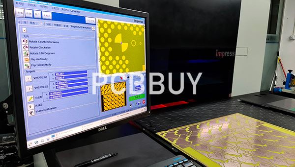
Data Comparison – The scanned image is compared against the original Gerber or CAD design files.
-
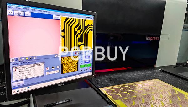
Defect Identification – Any discrepancies are automatically flagged, including trace width variations, solder bridges, or missing pads.
-
Engineer Verification – PCBBUY’s experienced quality engineers review the flagged points to confirm whether they are real defects or acceptable tolerances.
This systematic approach ensures that every board leaving our facility matches the customer’s design requirements.

AOI Inspection PCB Capabilities at PCBBUY
PCBBUY is equipped with state-of-the-art AOI equipment designed to detect even the smallest defects. Our AOI inspection PCB capabilities include:
-
High-Resolution Imaging – Detection accuracy at the micron level.
-
Support for Complex Boards – Suitable for multilayer PCBs, HDI designs, and BGA layouts.
-
Integration with Other Testing – AOI works in conjunction with flying probe testing and ICT (In-Circuit Testing) to provide both visual and electrical verification.
-
Compliance with Global Standards – Every PCB is inspected according to IPC-A-600 Class 2 and Class 3 requirements.
For example, in high-volume consumer electronics production, AOI enables us to deliver consistent results with minimal defect rates, while in medical and automotive projects, it ensures strict reliability standards are met.
AOI vs. Other PCB Inspection Methods
Different inspection methods play unique roles in PCB quality assurance. Below is a comparison:
|
Inspection Method |
Features |
Advantages |
Limitations |
|
AOI Inspection PCB |
Optical imaging |
Fast, accurate, non-destructive |
Cannot detect hidden defects |
|
Flying Probe Testing |
Electrical continuity |
Ensures net connectivity |
Slower for mass production |
|
X-Ray Inspection |
Penetration testing |
Detects hidden solder joints (e.g. BGA) |
Higher cost, slower process |
At PCBBUY, we integrate AOI with other inspection methods to create a comprehensive quality control system.
Why Choose PCBBUY for AOI Inspection PCB
Selecting the right manufacturing partner is crucial for ensuring product reliability. With over a decade of experience, PCBBUY stands out in AOI inspection PCB services due to:
-
Advanced AOI Machines – Capable of handling both prototype and mass production with precision.
-
Full Process Quality Control – From drilling, plating, impedance control, solder mask application, to final AOI inspection, every stage is monitored.
-
Custom Inspection Strategies – Tailored AOI parameters for different board designs, ensuring customer-specific requirements are met.
-
Global Export Experience – Trusted by international clients across Europe, North America, and Asia for high-end PCB solutions.

Conclusion
AOI inspection PCB is not just a step in manufacturing—it is the backbone of quality assurance. At PCBBUY, our commitment to precision and reliability ensures that every PCB undergoes rigorous AOI inspection before delivery. This process guarantees consistent performance, reduced defects, and higher customer satisfaction.
If you are looking for a PCB manufacturer with advanced AOI inspection PCB capabilities, PCBBUY is your trusted partner for high-quality, cost-effective, and reliable PCB solutions.
FAQ: AOI Inspection PCB
Q1: What defects can AOI inspection detect in PCB?
A1: AOI can detect missing pads, solder bridges, trace breaks, open circuits, short circuits, and solder paste defects.
Q2: Is AOI inspection necessary for every PCB?
A2: For high-density multilayer and fine-pitch designs, AOI inspection is essential to ensure product reliability and yield.
Q3: How does PCBBUY ensure quality with AOI inspection?
A3: By combining AOI with flying probe testing and strict IPC standards, PCBBUY ensures that all boards meet international quality requirements.
Industry Category


