Advanced Capabilities of a Leading HDI PCB Manufacturer
By:PCBBUY 06/13/2025 17:44

As the electronics industry demands increasingly compact, high-performance, and multi-layered designs, choosing a reliable HDI PCB manufacturer becomes critical. At PCBBUY, we specialize in manufacturing high-density interconnect (HDI) printed circuit boards using advanced techniques and stringent quality standards. Our capabilities ensure optimal performance in complex electronic applications, from mobile devices to aerospace systems.
In this article, we detail our comprehensive HDI PCB manufacturing capabilities, focusing on process specifications and material expertise that set us apart as a premier HDI PCB partner.
1. Material Engineering Excellence – Foundation of a Reliable HDI PCB Manufacturer
As an established HDI PCB manufacturer, PCBBUY selects high-grade base materials to meet diverse thermal and electrical demands. Our standard material is FR-4, with customization available including:
-
TG135-TG170 range laminates
-
Halogen-free options
-
CTI-compliant materials
This material flexibility enables us to support a wide variety of industrial applications, from automotive ECUs to 5G modules, where temperature resilience and dielectric stability are essential.

2. Multilayer Design from a True HDI PCB Manufacturer
Our multilayer HDI PCBs are fabricated with industry-leading precision. We support two core production stages:
-
1st Order HDI: 4–10 layers
-
2nd Stage HDI: 6–10 layers and above
Whether for compact handheld devices or high-layer-count server boards, PCBBUY ensures each layer is aligned with micrometer-level accuracy. Customization is also available for even more complex stackups.
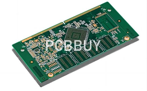
3. Construction Types of HDI PCB Manufacturer
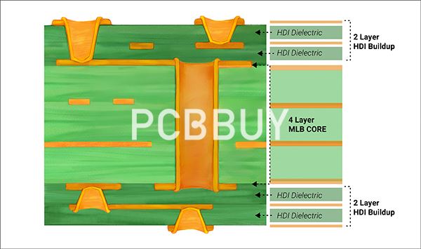
We accommodate both 1st and 2nd order HDI constructions with buried via support:
-
1st Order Examples: 1+N+1, 1+1+N+1+1 (with buried vias ≤0.3mm)
-
2nd Order Examples: 2+N+2, 1+2+N+2+1 (with buried vias ≤0.3mm)
Our internal mechanical via structures are recommended for high reliability, though we also support electroplated via filling when internal routing constraints apply. This flexibility positions PCBBUY as a responsive and capable HDI PCB manufacturer ready for custom engineering challenges.
4. Ultra-Fine Trace Width of HDI PCB Manufacturer
At PCBBUY, we meet the most demanding design rules with:
-
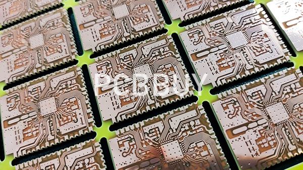
Minimum trace width: 2 mil (0.05mm)
This level of precision is made possible through advanced photolithography and etching control, enabling signal integrity even in the most densely packed HDI layouts.
5. Advanced Blind Via Processing at a Top HDI PCB Manufacturer
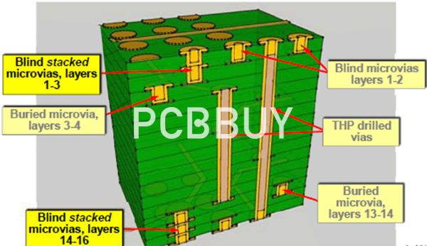
Blind vias are essential in HDI structures, allowing interconnection between outer and inner layers without impacting other layers. PCBBUY offers:
We utilize CO₂ and UV laser drilling for high precision, supported by strict depth control and alignment systems. Every blind via is inspected using X-ray metrology to ensure layer-to-layer consistency.
|
Minimum Hole Size |
|
|
Mechanical Blind Via |
≥0.15mm |
|
Laser Blind Via |
≥0.075mm |
We utilize CO₂ and UV laser drilling for high precision, supported by strict depth control and alignment systems. Every blind via is inspected using X-ray metrology to ensure layer-to-layer consistency.
6. Micro Hole Drilling and Copper Plating of HDI PCB Manufacturers
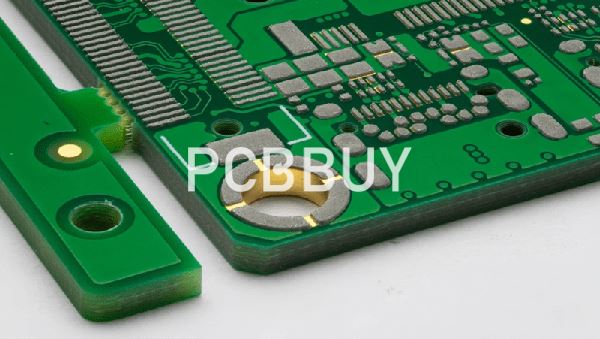
Our minimum unilateral hole size is ≥0.3mm, supporting a wide range of via types including microvia and via-in-pad applications. To ensure conductivity and structural reliability, PCBBUY uses:
-
>18μm copper thickness for mechanical holes (non-laser blind burial)
-
>13μm copper thickness for laser blind holes
These parameters exceed IPC Class 3 reliability standards, especially critical for mission-critical and medical applications.
7. Copper-Filled Via Electroplating of HDI PCB Manufacturer
PCBBUY employs a laser via electroplating process that includes:
-
Plating Depth Range: 0.05mm – 0.1mm
-
Tolerance: ±15%
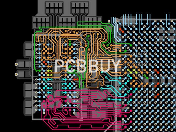
This process ensures full metallization of the via barrel. Copper is filled into the hole using controlled current density and bath chemistry, enabling via-in-pad flatness, ideal for BGA components and high-frequency signals.
Frequently Asked Questions (FAQ)
Q: What is the minimum trace width PCBBUY supports?
A: We support trace widths as small as 2 mil (0.05mm), ideal for compact and high-speed designs.
Q: Can PCBBUY handle via-in-pad designs for BGAs?
A: Yes, our copper-filled via electroplating ensures flat, reliable surfaces for via-in-pad BGA applications.
Q: What HDI constructions do you support?
A: We support 1st order (1+N+1) and 2nd order (2+N+2) HDI stackups with optional buried vias.
Q: What laser via sizes can be manufactured?
A: We can produce laser blind vias as small as 0.075mm in diameter.
Conclusion: Choose PCBBUY – The Trusted HDI PCB Manufacturer
At PCBBUY, our HDI PCB manufacturing capabilities are rooted in cutting-edge engineering, rigorous process control, and deep material knowledge. Our experienced team, state-of-the-art equipment, and customer-centric customization options make us the ideal partner for advanced HDI projects.
Whether you're developing wearable technology, IoT modules, or avionics systems, PCBBUY is your go-to HDI PCB manufacturer committed to delivering precision, performance, and peace of mind.
Industry Category


