All about HDI PCB Manufacturing Process with Analysis of PCB Industry
By:PCBBUY 01/20/2022 09:30

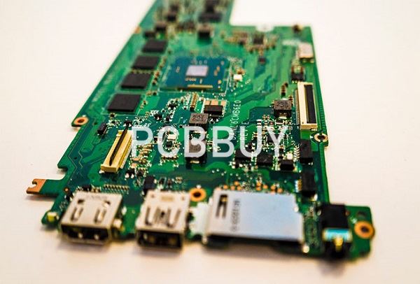
A HDI PCB is usually found in complex electronic devices that demand excellent performance while conserving space. Applications include mobile /cellular phones, touch-screen devices, laptop computers, digital cameras, 4/5G network communications, and military applications such as avionics and smart munitions.
In this passage, we are providing all the knowledge of HDI PCB, please check and read the content below for more information.
What is the market situation of HDI PCB?
Before we head into forecasts, let’s mention current statistics. It doesn’t take an expert to see that the printed circuit boards are trendy throughout the world. You can even find guides explaining how to make a PCB at home.
However, if you want to launch a commercial product, it is vital that you design and assemble a reliable PCB, and you need professional equipment and experts for that.
The PCB industry has recently set a new standard in high-density to interconnect technology (HDI). Users throughout the world have accepted it and implemented it in their products and other applications.
A report published by expert’s pinpoints that this market earned more than $9.4 billion in 2017. The estimation is that the compound annual growth rate (CAGR) will be over 11% in the coming years. If you do the math that means that the HDI PCB market can generate more than $22 billion by 2025!
That is not only 2.5 times more than the result made in 2017, but it is also an achievement that will positively surprise the entire industry. And the best part is that it seems more than feasible, especially if we consider the fantastic progress the sector made in only a couple of years.
Even if the growth is somewhat less than projected, There is no doubt that the high-density interconnect PCB market will usher in a bright future. The technology hasn’t reached its peak yet, which means we can expect even better boards in the coming years. On top of that, more companies are joining the production of HDI boards every day, increasing their use.

What is the process of HDI PCB manufacturing?
There are a number of steps involved in the typical PCB manufacturing process, but HDI PCB manufacturing uses some particular steps that may not used in other boards. The HDI design process starts like many other processes, where the
· Determine the layer count required to route all signals, either by using the largest BGA component on the board or by using the interface + direction count from the largest IC on the board.
· Contact your fabrication house to select materials and obtain dielectric data to create your PCB stackup.
· Based on layer count and thickness, determine the via style that will be used to route signals through inner layers.
· Perform a reliability assessment if relevant, to verify that the materials will not stress interconnects to fracture during assembly processing and operation.
· Determine design rules based on fabricator capabilities and reliability requirements (need for tear drops, trace widths, clearances, etc.) to ensure reliable manufacturing and assembly.
Stackup creation and determination of design rules are the critical points as they will determine ability to route the board and reliability of the end product. Once these points are completed, a designer can implement their fabricators DFM requirements and reliability requirements as design rules in their ECAD software. Doing this on the front-end is very important and it will help ensure the design is reliable, routable, and manufacturable.

Why HDI PCB is popular?
If we analyze the situation from 2017, we can notice that about 66% of the total HDI PCB revenue was for the tablet and smartphone industry. That makes sense because these products require a high-performing board that will be thin and compact-sized at the same time.
The experts do not doubt that smartphones and tablets will remain the most popular HDI PCB application in the coming years. They should keep the leading position for at least five years from now, but the exciting thing to discuss is the growing popularity of other smart products.
We are talking about smartwatches and other wearables with “smart” features. All those products are electronic devices, and they require printed circuit boards to work. As a result, the PCB industry has been producing significantly more for this application.
The estimated annual growth rate for PCB use for smart wearables is around 14% in the coming years. Although smartphones and tablets will remain at the top, watches and other wearables will get closer by 2025.
Industry Category


