BGA PCB Design Guidelines
By:PCBBUY 09/04/2021 09:20

BGA packages are used to permanently mount devices such as microprocessors. BGA is nothing but ball grid array which is a type of surface mount technology ( SMT ), and it means soldering between components and PCB. BGA consists of many overlapping layers that include one to a million multiplexers, logic gates, flip-flops or other circuits.
If you are interested in BGA of PCB design, you can follow us and read the content below for more information about it.
What are the rules of BGA PCB design?
The first step in BGA routing has nothing to do with routing, it’s all about determining the number of layers you’ll need for routing. For high-ball-count BGAs, the number of layers can get very high and the layer thickness can become very small in order to support the required number of traces with controlled impedance. Fortunately, there is a simple process you can use to estimate the number of signal layers required to fully breakout traces from your BGA.
· Count up the number of signal rows across the footprint of the largest BGA.
· Divide this number by 2 to get the total number of rows that will require breakout routing.
· Divide the number of breakout rows by 2 to get the number of signal layers required to support your signal rows.
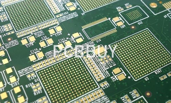
This formula is used because each layer can support 2 rows of traces, as shown in the image below. In this image, we have a 27-row BGA (found by counting the number of vias vertically). However, most of the internal rows (about 19) are for different power buses and ground connections. This leaves a total of 8 signal rows that will require routing; dividing this by 4 gives us 2 signal layers that are needed for breakout routing.
What are the advantages of BGA in PCB design?
With PCB BGA, you will get the following advantages:
BGA package eliminates the issue of developing small packages for ICs with lots of pins. Traditionally, dual-in-line and pin grid arrays surface-mount boxes had very little space between the pins. They provided a considerable disadvantage for the soldering process with more pins. However, you will not need to worry about accidentally soldering together two pins with BGA packages.

Again, when compared with packages with legs, The BGA package has a lower thermal resistance when placed on the PCB QUOTE. That permits the heat that IC produces in the box to conduct through the PCB efficiently. Of course, it will save your chip from overheating.
Do you know which property causes unwanted signals distortion in high-speed electronic circuits? The unwanted inductance in an electrical conductor is responsible for this phenomenon. However, BGAs have very little distance between PCB and the package, leading to lower lead inductance. Thus, you will get top-class electrical performance with pinned devices.
With BGAs, you can effectively utilize your printed circuit board space. You will be able to make connections right below the surface mount device (SMD). The links are no more limited to just the SMD package periphery.
Another advantage that will come with BGA is the reduced thickness of the package. That sounds great. You can quickly fabricate the PCBs in small electronic devices, such as smartphones.
Last but not least, you will get enhanced re-workability because of bigger pad sizes.
What are the challenges of BGA design for multilayer PCB?
The demand for compact electronics has spurred the development of electronics chips in the BGA form factor. Hundreds of signal and power pins are now littered underneath a smaller IC, compared to its QFP counterpart. It’s great news for marketers who promise tinier consumer products, but the nightmare for PCB designers is about to start.

Most of the BGAs would have a ball pitch between 0.5 mm to 1.0 mm. As the BGA package is usually meant for FPGA and microcontrollers, the number of pins underneath the IC could range between 200s to 2000. To make matters worse, the diameter of the balls decreases as the pitch gets smaller.
Fanning out the traces on a BGA chip and the manufacturing process is fraught with challenges. For example, a BGA chip with a 1.0 mm pitch and a 0.45 mm landing pad can be routed with a 0.18 mm trace on a channel. A channel in BGA routing means the space between two landing pads on the X or Y-axis.
Typically, squeezing a 0.18 mm trace between two 1.0 mm pitch is not an issue, except that BGA’s pads are arranged in a dense grid pattern. This means you’ll need to figure out how to connect the inner pads to their respective nets. The task gets much more complicated when you have a BGA with half the pitch size.
What are the considerations of BGA PCB design?
Define Appropriate Exit Routes
You may be having problems creating appropriate exit routes that don’t result in assembly failures or similar issues. For the right fan-out routing plan, you need to look into many PCB specifics, such as the number of I/O pins, pad and via size, trace width spacing, and how many layers are needed to fan out the BGA. Figure 6 illustrates exit paths in a BGA.
PCB BGA—Determining the Needed Layers
It will not be easy for you to decide the number of layers of a PCB layout as a designer. PCB with more layers will be expensive. On the other side, you may need to increase the number of layers to reduce noise.
First of all, you should determine the size of the via and the space and trace width of the PCB design. Then, it is also necessary to decide on the quantity of single-channel traces. After that, you should determine the number of layers that are required. For fewer layers, the critical point is to reduce the application of I/O pins.
Industry Category


