
How Does X-Ray Inspection Detect BGA Solder Joint Voiding?
By:PCBBUY 08/31/2026 17:24

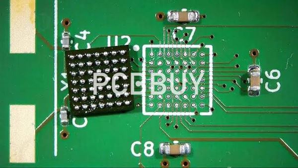
BGA packages provide high I/O density in a relatively small footprint, making them widely used in automotive electronics, industrial control systems, power electronics, energy storage equipment, and advanced robotic products. However, because BGA solder joints are hidden underneath the package, many soldering defects cannot be identified through conventional visual inspection.
This is where X-ray inspection for BGA solder joint voiding becomes particularly valuable.
From a PCB assembly engineering perspective, X-ray inspection is not simply a final quality check. It is an important process-control tool for evaluating hidden solder joints, identifying voids, and helping engineers determine whether a reflow process is producing consistent solder connections.
What Is BGA Solder Joint Voiding?
A solder void is an internal area within a solder joint where solder is replaced by gas or another non-metallic region. Voids can form during reflow when gases generated from solder paste flux, moisture, contamination, or other sources become trapped before the solder solidifies.
A small amount of voiding may occur naturally in some soldering processes. The engineering concern is not simply whether a void exists, but its size, location, distribution, and effect on the electrical and thermal function of the joint. This is especially important for BGA devices used in applications where solder joints may experience thermal cycling, mechanical stress, or significant heat dissipation requirements.

Why Can't Conventional AOI Reliably Detect BGA Voids?
AOI is highly effective for inspecting visible soldering and component-placement conditions. However, a BGA package physically covers the solder joints. As a result, AOI generally cannot directly inspect the internal structure of a BGA solder ball after assembly.
X-ray inspection provides a different perspective by using X-rays to create an image based on differences in material absorption. This makes it possible to inspect solder joints hidden underneath BGA packages without removing the component.
X-Ray vs. AOI for BGA Inspection
|
Inspection Method |
What It Can Inspect |
BGA Internal Voids? |
|
AOI |
Component placement, visible solder joints, solder paste-related surface defects |
Generally not directly visible |
|
X-ray inspection |
Hidden solder joints, voids, bridging and internal solder distribution |
Yes |
|
Electrical testing |
Electrical connectivity and certain functional conditions |
Cannot directly identify physical voids |
|
Visual inspection |
External component and soldering appearance |
No for hidden BGA joints |
For a PCBA containing both conventional components and BGAs, these inspection methods are complementary rather than interchangeable.
How Does X-Ray Inspection Detect BGA Voiding?
During X-ray inspection, the assembled PCB is positioned so that the X-ray system can generate an image of the BGA area. Because solder and other materials attenuate X-rays differently, variations inside the solder joints can appear as contrast differences in the X-ray image.
A trained engineer can use the image to evaluate characteristics such as:
-
Presence of internal voids
-
Approximate void size and distribution
-
Solder bridging
-
Missing or abnormal solder connections
-
BGA ball alignment
-
Certain internal assembly defects
For more advanced inspection systems, image-processing software can assist with identifying and measuring void-related features. However, automated measurement does not eliminate the need for appropriate engineering judgment and acceptance criteria.

What Causes Voids in BGA Solder Joints?
BGA voiding is usually related to the interaction between solder paste, PCB design, component characteristics, and the reflow process.
Common contributing factors include:
1. Flux and Volatile Materials
Solder paste contains flux and other materials that can release gases during heating. If these gases cannot escape before solder solidification, they may become trapped inside the joint.
2. Reflow Profile
An unsuitable reflow profile can affect flux activation, solvent evaporation, solder melting, and solidification. Important parameters include heating rate, soak behavior, peak temperature, time above liquidus, and cooling rate. For this reason, the reflow profile should be established according to the solder paste manufacturer's recommendations and the thermal characteristics of the actual assembly.
3. Solder Paste Printing
Printing quality directly influences the amount and distribution of solder paste deposited onto BGA pads. Poor stencil design, insufficient paste release, excessive paste volume, or inconsistent printing can increase soldering variation and contribute to voiding or other BGA defects.
4. PCB and Component Moisture
Moisture can become a source of vapor during reflow. Proper storage and handling of moisture-sensitive components and PCB materials are therefore important for reliable assembly.
5. Pad and Stencil Design
BGA pad geometry, stencil aperture design, paste volume, and thermal design can influence how gases escape from the molten solder. For some high-reliability or thermal applications, engineers may need to optimize the stencil design and reflow process together rather than attempting to solve voiding through one parameter alone.
Why Does BGA Void Location Matter?
The location of a void can be as important as its overall size. A void positioned near a critical interface or concentrated in a thermally important region may have a different impact from several smaller, distributed voids.
For power components, thermal performance deserves particular attention. If a solder joint or thermal pad provides an important heat-transfer path, excessive voiding can increase thermal resistance and affect heat dissipation. Therefore, engineers should avoid evaluating BGA voiding based solely on a single percentage without considering:
-
Component function
-
Solder joint geometry
-
Void size and distribution
-
Thermal requirements
-
Electrical requirements
-
Mechanical reliability
-
Applicable customer or industry specifications
How Can PCBBUY Help Control BGA Assembly Quality?
For BGA assemblies, controlling defects starts before X-ray inspection.
PCBBUY's SMT assembly capabilities include solder paste printing, high-speed pick-and-place, double-sided placement, reflow soldering, AOI inspection, and other assembly processes.
Its SMT process equipment includes a 10-zone reflow oven with temperature control capability of approximately ±1°C, while the placement process supports high-speed component placement with equipment specifications reaching 45,000 placements per hour and ±30 μm placement accuracy.
These capabilities help provide a controlled manufacturing environment for fine-pitch and high-density assemblies.
For BGA applications, process control can include:
-
Reviewing PCB pad and component information before production.
-
Selecting an appropriate stencil and solder paste process.
-
Controlling solder paste printing consistency.
-
Establishing and verifying the reflow profile.
-
Performing AOI for visible assembly defects.
-
Applying X-ray inspection where hidden solder joints require verification.
-
Reviewing abnormal X-ray results and adjusting the process when necessary.
-
Performing electrical tests according to the project requirements.
PCBBUY also supports PCB fabrication capabilities such as HDI, high-layer-count boards, controlled impedance, copper thickness customization, and via filling, which can be important when the BGA assembly is part of a dense or high-performance PCB design.
What Should Be the Acceptance Standard for BGA Voiding?
There is no single void percentage that should automatically be applied to every BGA assembly. The acceptable level depends on the applicable IPC requirements, customer specifications, component manufacturer's recommendations, soldering process, and the functional role of the solder joint.
For critical automotive, industrial-control, power, energy-storage, and robotic electronics, the inspection criteria should ideally be agreed upon before production. This is particularly important when the BGA is also involved in heat transfer or when the product will experience substantial thermal cycling.
How Can X-Ray Results Improve the Reflow Process?
One of the biggest advantages of X-ray inspection is that it can provide feedback to the manufacturing process. For example, if X-ray images show a consistent increase in voiding across multiple BGA joints, engineers can investigate the solder paste, stencil, PCB surface, component condition, and reflow profile.
If voiding is concentrated in a particular area, the investigation can focus on local thermal conditions, pad geometry, solder volume, or board/component design. This makes X-ray inspection more useful as a process-improvement tool, rather than simply a pass/fail inspection performed at the end of production.
Conclusion
X-ray inspection for BGA solder joint voiding is an important technique for evaluating solder joints that cannot be visually inspected after assembly. It can reveal internal voids and other hidden conditions, helping manufacturers identify process variation that may otherwise remain undetected.
However, X-ray inspection should not be treated as a substitute for good process engineering. Reliable BGA assembly depends on solder paste printing, stencil design, component handling, PCB design, reflow-profile control, inspection, and electrical testing working together.
For demanding applications such as automotive electronics, industrial controls, power systems, energy storage, and embodied robotics, PCBBUY combines PCB fabrication and SMT assembly capabilities to support high-density and reliability-focused PCBA projects. Project-specific X-ray inspection criteria can be established according to the PCB design, component requirements, customer specifications, and applicable industry standards.
FAQ
1. Can X-ray inspection detect BGA solder joint voids?
Yes. X-ray inspection can reveal internal voids within BGA solder joints because the solder and void regions produce different X-ray attenuation characteristics.
2. Can AOI detect BGA solder joint voiding?
Generally, no. Because BGA solder joints are hidden underneath the component package, conventional AOI cannot directly inspect internal voids. X-ray inspection is more suitable for this purpose.
3. What causes BGA solder joint voiding?
Common contributing factors include solder paste flux volatiles, moisture, stencil and paste-printing conditions, pad design, component characteristics, and the reflow profile.
4. Are BGA solder voids always a reliability problem?
Not necessarily. Some degree of voiding can occur naturally during reflow. The engineering significance depends on factors such as void size, location, distribution, solder-joint function, thermal requirements, and applicable acceptance criteria.
5. Does PCBBUY provide X-ray inspection for BGA assemblies?
For BGA and other hidden solder-joint applications, the appropriate inspection method and requirements should be confirmed with PCBBUY based on the specific PCBA project. PCBBUY supports SMT assembly and multiple PCB/PCBA quality-control processes, including AOI and electrical testing.
6. How can BGA voiding be reduced?
Start with the complete process rather than changing only the reflow temperature. Review solder paste, stencil aperture design, paste volume, PCB/component moisture handling, pad design, and the reflow profile. X-ray inspection can then be used to verify whether the process changes produce more consistent solder joints.
Industry Category








