
What Is Back Drilling in PCB Manufacturing and Why Is It Used?
By:PCBBUY 09/18/2026 14:16
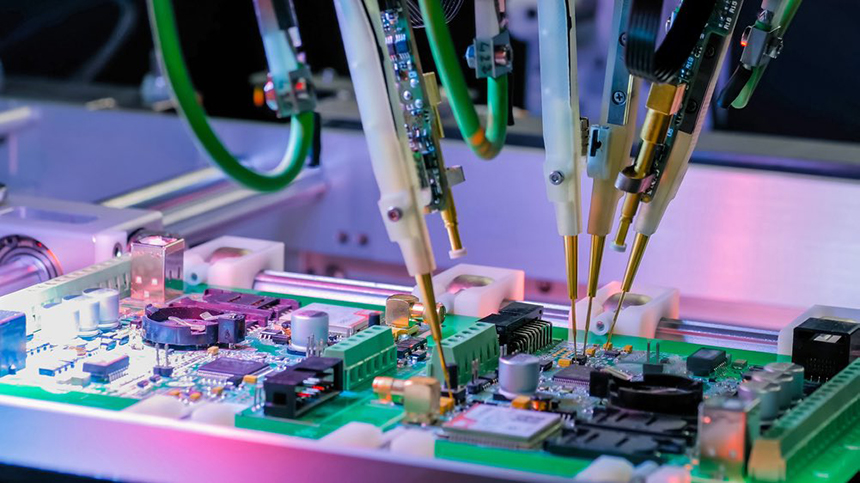
As data rates increase, maintaining signal integrity becomes more challenging, particularly in multilayer PCBs with long plated through-holes. Although through-hole vias provide reliable electrical connections between PCB layers, the unused portion of a via can negatively affect high-speed signal transmission.
Back drilling, also known as controlled-depth drilling or controlled-depth backdrilling, is a PCB manufacturing technique used to remove this unwanted portion of the plated via barrel. It is commonly considered for high-speed digital circuits, backplanes, communication equipment, and other applications where signal integrity is critical.
For automotive electronics, industrial control systems, power electronics, and advanced energy-related equipment, understanding when and how to apply back drilling can help designers balance electrical performance, manufacturing feasibility, and cost.
What Is Back Drilling in PCB Manufacturing?
Back drilling is a secondary drilling process that removes the unused section of a plated through-hole after the conventional through-hole drilling and plating processes have been completed.
A standard plated through-hole may extend through the entire PCB, even though the signal only needs to travel between certain layers. The portion of the copper barrel that extends beyond the last layer used by the signal is called a via stub.
When a high-speed signal passes through the via, the unused stub can behave like an unwanted transmission-line branch. Depending on the signal rise time, frequency content, stub length, and PCB stackup, it may cause signal reflections, resonance, impedance discontinuities, and signal loss.
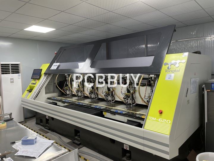
During back drilling, a drill with a diameter slightly larger than the original via is used to remove most of the unused copper barrel from the opposite side of the PCB. The drilling depth is carefully controlled so that the required electrical connections remain intact.

How Does the PCB Back Drilling Process Work?
Back drilling does not replace conventional through-hole fabrication. Instead, it is an additional operation performed after the plated through-hole has been formed.
The typical process includes the following stages:
1. Conventional Through-Hole Drilling and Plating
The PCB is drilled and plated using the standard manufacturing process. This creates a continuous copper barrel through the required board thickness.
2. Back Drill Positioning
The manufacturer identifies the vias that require stub removal and aligns the back-drilling tool with the existing holes.
3. Controlled-Depth Re-Drilling
A larger drill is used to remove the unwanted plated barrel from the selected side of the board. The drill stops before reaching the layer that must remain electrically connected.
4. Residual Stub Control
A small residual stub is generally left to avoid damaging the functional pad, barrel, or connection layer. The target residual stub length should be defined according to the signal-integrity requirements and the manufacturer’s process capability.
5. Inspection and Verification
The back-drilled structure should be checked according to the agreed manufacturing requirements. For demanding applications, cross-section analysis or other suitable verification methods may be considered.
Why Is Back Drilling Important for High-Speed PCBs?
A long via stub can introduce an unwanted discontinuity into a high-speed signal path. Its impact depends on the electrical length of the stub rather than simply the nominal data rate.
Potential effects include:
-
Increased signal reflection
-
Return-loss degradation
-
Insertion-loss deterioration
-
Resonance at specific frequencies
-
Eye-diagram closure
-
Timing distortion and jitter
-
Reduced high-speed channel margin
Back drilling reduces the length of the unused via barrel and therefore helps minimize these effects.
However, back drilling is not automatically required for every high-speed PCB. Designers should evaluate the complete channel, including the signal rise time, stackup, via geometry, operating frequency, impedance requirements, and simulation results.
Back Drilling Compared with Other Via Structures
Back drilling is only one method of controlling via-related signal discontinuities. Depending on the board structure and project requirements, designers may also consider blind vias, buried vias, microvias, or an optimized layer stackup.
|
Via or Structure |
Main Feature |
Typical Consideration |
|
Standard through-hole via |
Extends through the board and connects multiple layers |
Economical and mechanically robust, but may create long via stubs |
|
Back-drilled via |
Removes most of the unused plated barrel |
Helps reduce stub-related signal discontinuities |
|
Blind via |
Connects an outer layer to one or more internal layers |
Can reduce unnecessary via length but may require more complex fabrication |
|
Buried via |
Connects internal layers without reaching the outer surface |
Useful for high-density multilayer designs, but increases manufacturing complexity |
|
Microvia |
Small-diameter, usually laser-drilled interconnection |
Suitable for HDI designs and compact routing structures |
The most appropriate solution depends on the electrical requirements, layer count, available space, manufacturing process, and target cost.
PCB Back Drilling: Important Design Considerations
To improve manufacturability, the back-drilling requirements should be clearly defined in the fabrication data or engineering drawing.
Designers should communicate the following information to the PCB manufacturer:
-
The specific vias that require back drilling
-
The back-drilling entry side
-
The target stop layer or permitted drilling depth
-
The required residual stub length
-
The back-drill diameter
-
Clearance requirements around the back-drilled holes
-
Any special inspection or documentation requirements
The back-drill diameter must be large enough to remove the unwanted copper barrel, but it should not damage nearby traces, planes, pads, or other structures.
It is also important to avoid specifying an arbitrary drilling depth without considering the actual finished board thickness and dielectric thickness. A layer-based drilling requirement can be more practical because material thicknesses may vary during PCB fabrication.
How Can PCBBUY Support Complex PCB Manufacturing Requirements?
For automotive electronics, industrial control systems, power equipment, energy storage systems, new-energy applications, and embodied robotics, PCB designs often require a combination of high layer counts, controlled impedance, high-density interconnections, and specialized drilling structures.
PCBBUY’s PCB manufacturing capabilities include:
-
Large-size PCB production: Maximum production size of 1000 × 600 mm
-
HDI manufacturing: Support for first-order and second-order HDI structures
-
Laser-drilled blind vias: Minimum laser-drilled blind via diameter of Φ0.075 mm
-
Mechanical blind vias: Minimum mechanically drilled blind via diameter of Φ0.15 mm
-
Controlled-depth drilling for specialized structures: Controlled-depth drilling accuracy of ±15 μm for applicable step-hole and slot processes
-
High-frequency and high-speed materials: Support for materials from Rogers, TUC, Isola, and other manufacturers
-
Mixed-material lamination: Support for asymmetric and heterogeneous mixed-material lamination
-
Quality control: AOI, flying-probe testing, and four-wire low-resistance testing
These capabilities can support the development of complex multilayer and high-speed PCB projects. For a design that specifically requires back drilling, the engineering team should review the complete Gerber files, stackup, drill files, back-drill specifications, and required tolerances before production. Back-drilling availability and project-specific process limits should be confirmed during the engineering review.
Conclusion
Back drilling in PCB manufacturing is a controlled-depth drilling process used to remove unwanted via stubs from plated through-holes. By shortening the inactive portion of a via, it can help reduce signal reflections and improve signal integrity in demanding high-speed designs.
However, back drilling should be selected based on the actual electrical requirements of the design rather than used as a universal solution. Clear drilling instructions, suitable layer-stack planning, adequate copper clearances, and communication with the PCB manufacturer are essential for achieving reliable results.
For complex applications such as automotive electronics, industrial control, power systems, energy storage, and embodied robotics, early engineering evaluation can help determine whether back drilling, HDI structures, or another interconnection strategy is the most appropriate choice.
FAQ
1. What is back drilling in PCB manufacturing?
Back drilling is a controlled-depth secondary drilling process used to remove the unused plated portion of a through-hole via, also known as a via stub.
2. Why are via stubs a problem in high-speed PCBs?
Long via stubs can behave like unwanted transmission-line branches and may cause signal reflections, resonance, insertion-loss degradation, and other signal-integrity problems.
3. Does back drilling remove the entire via stub?
Not usually. A small residual stub is generally left to protect the required electrical connection and avoid damaging the functional pad or barrel.
4. Is back drilling necessary for every high-speed PCB?
No. The need for back drilling depends on the signal rise time, operating frequency, via-stub length, stackup, channel design, and signal-integrity margin.
5. Is back drilling the same as blind-via fabrication?
No. Back drilling removes the unwanted portion of an already plated through-hole. A blind via is manufactured to connect an outer layer with selected internal layers without extending through the entire board.
6. What information should be provided for a back-drilling project?
The design package should specify the required vias, entry side, stop layer or drilling depth, residual stub target, back-drill diameter, and relevant clearance and inspection requirements.
7. Can PCBBUY manufacture PCBs with complex via structures?
PCBBUY supports multilayer PCB manufacturing, first-order and second-order HDI structures, laser-drilled blind vias, mechanical blind vias, and specialized controlled-depth drilling processes. Specific back-drilling requirements should be confirmed through engineering review before production.
Industry Category








