Benefits, Process, and Tolerance Capabilities ENEPIG PCB Finish
By:PCBBUY 07/25/2025 15:05
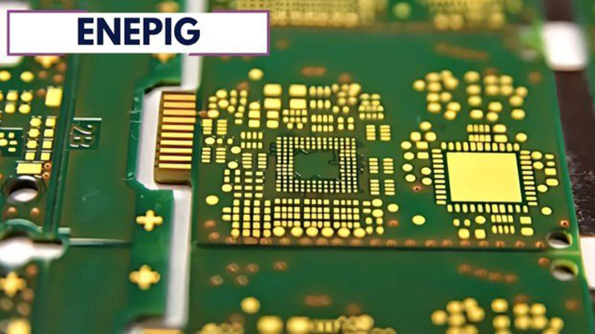
In the world of advanced PCB manufacturing, ENEPIG PCB finish (Electroless Nickel Electroless Palladium Immersion Gold) has become a gold standard for high-reliability and high-performance surface treatments. Known for its excellent wire bonding capabilities, superior solderability, and resistance to corrosion, ENEPIG is widely used in applications ranging from aerospace to data centers.
At PCBBUY, we specialize in manufacturing high-quality PCBs with ENEPIG surface finishes, offering precise thickness control, scalable production, and full process traceability.
Understanding the ENEPIG PCB Finish Process
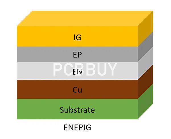
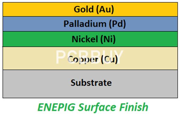
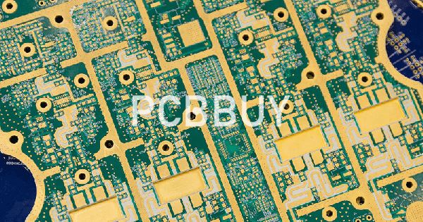
ENEPIG is a multi-layer metal surface finish applied to exposed copper pads. The process involves three critical steps:
-
Electroless Nickel (Ni) – Provides a strong, corrosion-resistant barrier and a foundation for further plating.
-
Electroless Palladium (Pd) – Acts as a diffusion barrier to prevent nickel from reacting with the gold layer, and ensures superior wire bonding.
-
Immersion Gold (Au) – Offers excellent oxidation resistance and a solderable surface for component attachment.
This combination allows ENEPIG to support both aluminum and gold wire bonding, making it the most versatile surface finish in the industry.

PCBBUY’s ENEPIG PCB Finish Specifications
At PCBBUY, we follow industry-leading standards while offering flexibility to meet custom requirements.
|
Material |
Thickness Standard |
Notes |
|
Nickel (Ni) |
200µ" (standard) |
Max allowed: 300µ" |
|
Palladium (Pd) |
1–10µ" |
Max total Pd+Au ≤ 30µ" |
|
Gold (Au) |
1–10µ" |
Excellent surface solderability |
Special thickness requests can be accommodated upon evaluation. Every ENEPIG batch at PCBBUY undergoes precise thickness testing using X-ray fluorescence (XRF) inspection tools.
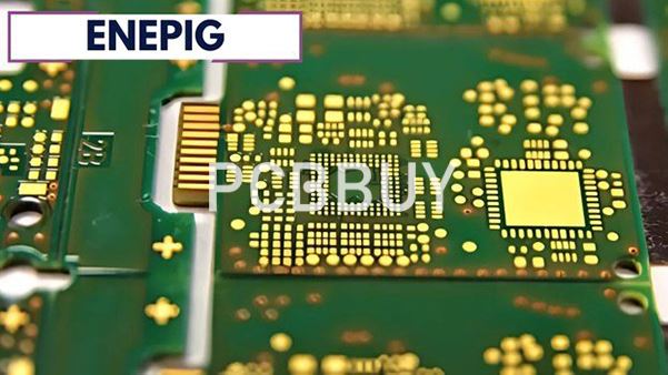
ENEPIG PCB Finish Manufacturing Flow at PCBBUY
Our advanced production line ensures consistent quality across every panel. Here's a simplified overview of the ENEPIG process flow:
-
Surface Preparation – Microetching and cleaning of exposed copper
-
Electroless Nickel Plating – Depositing Ni layer (200µ" ±10%)
-
Electroless Palladium Plating – Controlled Pd deposition (1–10µ")
-
Immersion Gold Plating – Final Au layer (1–10µ")
-
Surface Inspection – Thickness verification & adhesion tests
-
Packaging and Shipping – Moisture-sensitive packaging available
All steps are RoHS compliant, and we offer documentation upon request, including XRF reports and surface morphology scans.
Why Choose ENEPIG PCB Finish from PCBBUY?
|
Feature |
PCBBUY ENEPIG Capability |
|
Thickness Control |
±10% (XRF measured) |
|
Surface Uniformity |
Excellent |
|
Wire Bonding |
Gold & Aluminum |
|
Black Pad Risk |
None |
|
RoHS & REACH |
Fully Compliant |
|
Minimum Line Width/Spacing |
≤3mil available |
|
Support |
One-on-one engineering support |
PCBBUY uses automated chemical dosing systems and inline thickness monitors, ensuring repeatability and reliability across small and large volume runs.
📊 ENEPIG vs ENIG vs OSP: A Comparative View
|
Feature |
ENEPIG |
ENIG |
OSP |
|
Wire Bonding |
✅ |
❌ |
❌ |
|
Solderability |
✅ |
✅ |
✅ |
|
Anti-Oxidation |
✅ |
✅ |
❌ |
|
Black Pad Risk |
❌ |
✅ |
❌ |
|
Cost |
💲💲💲 |
💲💲 |
💲 |
|
Application |
High-End |
General |
Low-Cost |
ENEPIG outperforms ENIG and OSP in environments requiring high frequency, thermal cycling durability, or fine-pitch IC packaging.
Applications That Benefit from ENEPIG PCB Finish
-
Aerospace systems
-
Medical diagnostic devices
-
Networking equipment
-
Wire-bonded chip packaging
-
Military-grade electronics
-
Automotive radar & control units
ENEPIG finish provides both mechanical durability and electrical reliability, even in harsh environments.

Choose PCBBUY for Your Next ENEPIG PCB Project
With years of experience serving clients globally, PCBBUY is your trusted partner for ENEPIG PCB manufacturing. Whether you're prototyping or scaling to mass production, our engineering team is ready to assist with DFM reviews, custom finish specs, and fast turnaround times.
Request a quote today or upload your Gerber files to get started with high-performance ENEPIG PCB finish solutions tailored to your application.
FAQs About ENEPIG PCB Finish
Q1: Can ENEPIG be used for BGA or QFN packages?
Yes, ENEPIG provides a flat, solderable surface suitable for BGA, QFN, and CSP.
Q2: Is ENEPIG more expensive than ENIG?
Yes, but it offers significantly better performance for demanding applications.
Q3: What is the shelf life of an ENEPIG PCB?
Typically up to 12 months if vacuum-packed and stored properly.
Industry Category


