Benefits of multilayer PCB
By:PCBBUY 07/05/2021 17:30

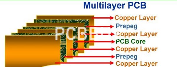
A PCB is considered multilayer when it has three or more layers with conductive copper foil. The layers are circuit boards with two sides that have been laminated and then glued together. They also include insulation between the layers to help protect the boards from heat. The electronic connections that take place between the layers happen through vias. These might be blind vias, buried vias, or with plating through holes in the board. This allows for there to be more connections and can make for complex printed circuit boards.
The multilayer PCBs became essential when the need for more sophisticated electronics rose. The standard PCBs were not capable of handling the needs of the new electronics because there would often be issues with stray capacitance, crosstalk, and noise. The multilayer PCB can help to deal with those issues. The number of layers that are used in these boards will vary. Typically, applications will require between four and eight layers, but it depends on several factors.
Why to choose multilayer PCB?
These types of PCBs offer a range of benefits. One of the most common reasons for using the multilayer PCB is the size. Because of the layered design, it means that the PCB will be smaller than other printed circuit boards but still have the same level of functionality. Most people today want their electronics to be smaller, while still being powerful. The multilayer PCB allows for this. These types of boards also happen to weigh less, which helps to reduce the overall weight of the gadgets in which they are used. However, the size is certainly not the only benefit.
Typically, these boards will also be high-quality and very reliable. A lot of work goes into the design of the boards to ensure they will work. When combined with quality materials and construction, they can last. They are known for being durable, and a big part of this is the insulation layers that are between the board layers.
The connections on these boards are closer together than they are on standard PCBs. This means that they tend to be more connective and more powerful. They will have a greater capacity, as well as improved speed. The multilayer PCBs also have just a single connection point. This is helpful in the design of the final product in which they will be used. It will mean that the product only needs to have a single connection point. This allows for more design freedom for those gadgets.
These are some of the biggest benefits of multilayer PCBs. If you aren’t already considering using them for your next design, it might be time that you thought about it.
Benefits of multilayer PCB
From a technical point of view, multilayer PCBs present several advantages in design. These benefits multilayer PCBs present include:
· Small Size: One of the most prominent and lauded benefits of using multilayer PCBs lies in their size. Because of their layered design, multilayer PCBs are inherently smaller than other PCBs with similar functionality. This presents a major benefit to modern electronics, as the current trend is working toward smaller, more compact yet more powerful gadgets like smartphones, laptops, tablets and wearables.
· Lightweight Construction: With smaller PCBs comes less weight, especially as the multiple connectors required to interlink separate single and double-layered PCBs are eliminated in favor of a multilayered design. This, again, is beneficial for modern electronics, which are geared more toward mobility.
· High-Quality: Due to the amount of work and planning that must go into the creation of multilayer PCBs, these types of PCBs tend to be better in quality than single and double-layer PCBs. They also tend to be more reliable as a result.
· Increased Durability: Multilayer PCBs tend to be durable by their nature. Not only do these multilayer PCBs have to withstand their own weight, but they must also be able to handle the heat and pressure used to bind them together. On top of these factors, multilayer PCBs use multiple layers of insulation between circuit layers, binding it all together with prepreg bonding agent and protective materials.
· Enhanced Flexibility: Though this does not apply to all multilayer PCB assemblies, some do use flexible construction techniques, resulting in a flexible multilayer PCB. This can be a highly desirable trait for applications where mild bending and flexing may occur on a semi-regular basis. Again, this does not apply to all multilayer PCBs, and the more layers incorporated into a flexible PCB, the less flexible the PCB becomes.
· More Powerful: Multilayer PCBs are extremely high-density assemblies, incorporating multiple layers into a single PCB. These close-quarters enable boards to be more connective, and their innate electrical properties allow them to achieve greater capacity and speed despite their smaller size.
· Single Connection Point: Multilayer PCBs are designed to work as a singular unit, rather than in tandem with other PCB components. As a result, they have a single connection point, rather than the multiple connection points required to use multiple single layer PCBs. This proves to be a benefit in electronic product design as well since they only need to include a single connection point in the final product. This is particularly beneficial for small electronics and gadgets designed to minimize size and weight.
These benefits make multilayer PCBs highly useful in a variety of applications, particularly mobile devices and high-functioning electronics. In turn, with so many industries turning to mobile solutions, multilayer PCBs are finding a place in an increasing number of industry-specific applications.
Industry Category


