Buried via VS blind via
By:PCBBUY 07/06/2021 17:19

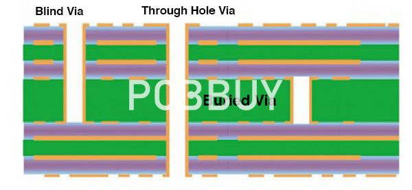
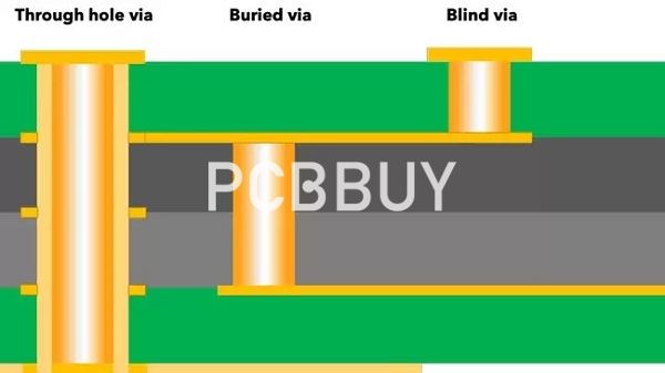
A via is simply a hole, drilled or plated, that is in the PCB that will allow a signal to pass to the inner layer of the board or to the other side of the board. Vias often connect component leads to planes or signal traces. These allow a change to the signal layers. If the via goes completely through the PCB board, it is often called a through-via. You might also hear people refer to this as a through-hole.
Blind and buried vias are only available on boards that have at least four layers. They connect the inner layers with other inner layers that are adjacent to them or to adjacent surface layers. And in this passage we will talk about the differences between buried via and blind via. Come and check for the more professional information of them.
If you want to order PCB product, please check and custom your order online.
What is blind via?
When examining blind and buried vias, there are several different types of blind vias to be considered. There are photo-defined blind vias, controlled-depth blind vias, sequential-lamination blind vias, and laser-drilled blind vias.
· Photo-defined blind vias. The creation of photo-defined blind vias requires laminating a photosensitive resin to a core. The photosensitive sheet will have a pattern on it that indicates the areas where the holes will be made. It is then exposed to light that causes the remaining material on the board to harden. The PCB is then put into an etching solution that removes the material from the holes that were created, which creates pathways. Copper is then plated in the hole and on the outer surface, which creates the outer layer of the PCB.
· Controlled-depth blind vias. The creation of controlled-depth blind vias is very similar to creating through-hole vias. The only difference is that the drill used to make the holes is set so that it will only go partially through the PCB. Modern technology makes it possible to do this accurately so that the features below the hold will not come into contact with the drill. Once the hole is drilled, it will then be plated in copper. This is the least expensive option, but it does require that the holes are large enough that they can be made with a drill. While this will work for many PCB needs, it might not always be the right solution for everyone.
· Sequential-lamination blind vias. Sequential-lamination blind vias are created using a piece of laminate that is extremely thin. The process is similar to creating a two-sided PCB, where the laminate will be drilled, plated, then etched. This method creates elements in the side that will form the second layer of the board. On the other side will be a copper sheet, which forms the first layer. This assembly is then laminated with the other layers of the board before going through the remaining steps to becoming a complete PCB. This method is not used as much today as it was in the past, because it is expensive.
· Laser-drilled blind vias. Laser-drilled blind vias are made after the PCB has been laminated, but before the outer layer undergoes etching and lamination. There are different types of lasers used to make the holes today, but the results are the same.
What is buried via?
When a via goes between two inner layers of a PCB but does not touch the surface of either side, it is called a buried via. Buried vias create connections between the inner layers. As the name suggests, vias are literally “buried” within the PCB. The functionality of a buried via is similar to that of a blind via, as the goal is to make sure that the PCB has the full functionality that is required. Buried vias help free up space in other areas of the board. To create buried vias, the inner layers with the vias are created first, and then other layers are added to the outside to build up the board.
What are the differences between buried via and blind via?
A blind via will connect an outer layer of the board to one of the inner layers. However, it does not go all the way through the entire PCB. A buried via is located within the board and will connect the inner layers without reaching the outer layers. There is also a through-hole, which goes through the entire board vertically and will connect all the layers. It is a relatively simple concept to understand, and it can provide some excellent benefits.
Benefits of buried via and blind via
Many PCB boards are small and have a limited amount of space, so the blind and buried vias can provide additional room and options for the board. The buried vias, for example, will help to free up space on the surface of the board without affecting the surface components or traces that are on the top or bottom layers. The blind vias can help to free up some additional space. They are often used for fine pitch BGA components. Since the blind vias only go through a portion of the board, it also means that there will be a reduction of signal stubs.
While the blind and buried vias can be used with many various PCBs, they tend to be used most often for high-density interconnect PCBs, or HDIs. The HDIs are popular because they can offer better power delivery and an added layer density. Through the use of the hidden vias, it will also help to keep the board smaller and lighter, which is very helpful when you are creating electronics. They are commonly used in medical devices, tablets, laptops, cellphones, and similar small electronics.
While the blind and buried vias can be helpful for those who need them, they can also add to the cost of the PCB. This is due to the added work that is required to add them to the board, along with the testing and manufacturing that will need to go into them. This means that you should only use them when it is truly necessary; because you want to have a great board that is tight and efficient.
Wanna know PCB knowledge? Check and read for more.
Industry Category


