
PCB Surface Roughness Effects on High-Speed Signal: Why Copper Profile Matters in PCB Design
By:PCBBUY 07/29/2026 16:56
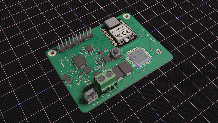
As digital communication speeds continue to increase, PCB designers are paying closer attention to factors that were once considered negligible. One of these critical factors is PCB surface roughness, which directly influences signal integrity, insertion loss, impedance stability, and overall system reliability.
In high-speed applications such as 5G infrastructure, AI servers, data centers, automotive radar, aerospace electronics, and high-frequency RF systems, even microscopic variations in copper surface profile can significantly affect signal transmission.
Understanding the PCB surface roughness effects on high-speed signal helps engineers optimize PCB stackups, select suitable materials, and choose manufacturers capable of controlling copper treatment throughout the fabrication process.
As an experienced manufacturer of high-precision multilayer and HDI PCBs, PCBBUY combines advanced material selection, precision etching, impedance control, and strict quality inspection to produce PCBs optimized for high-speed signal performance.
What Is PCB Surface Roughness?
PCB surface roughness refers to the microscopic texture of copper conductors after foil manufacturing, chemical treatment, etching, and surface preparation.
Although copper appears smooth to the naked eye, under microscopic inspection it contains peaks and valleys that increase the actual conductor surface area.
For low-frequency circuits this has little effect. However, at multi-gigahertz frequencies, high-speed signals travel primarily along the conductor surface due to the skin effect, making copper roughness an important contributor to signal loss.
|
Copper Surface Characteristic |
Description |
|
Smooth Copper |
Lower conductor loss and better signal integrity |
|
Standard Copper Profile |
Balanced adhesion and electrical performance |
|
Rough Copper |
Increased conductor loss at high frequencies |
|
Ultra-Low Profile (ULP) Copper |
Optimized for high-speed digital and RF applications |
Why Surface Roughness Affects High-Speed Signals?
As operating frequency increases, current distribution shifts toward the outer surface of the conductor.
Because of the skin effect:
-
Current flows through a much thinner conductive layer.
-
Surface irregularities increase the effective current path.
-
Electrical resistance rises.
-
Signal attenuation becomes more significant.
This results in greater insertion loss and degraded signal quality.
|
Frequency Range |
Surface Roughness Impact |
|
Below 500 MHz |
Minimal |
|
1–5 GHz |
Moderate |
|
10–28 GHz |
Significant |
|
Above 28 GHz |
Critical for signal integrity |
Major Effects of PCB Surface Roughness on High-Speed Signal Performance
1. Increased Insertion Loss
Insertion loss measures how much signal power is lost during transmission.
Rough copper increases conductor resistance, causing additional attenuation.
|
Surface Condition |
Signal Loss |
|
Smooth Copper |
Lowest |
|
Standard Copper |
Moderate |
|
Rough Copper |
Higher |
|
Oxidized Rough Surface |
Highest |
For PCIe Gen5/Gen6, USB4, Ethernet 112G, and high-speed SerDes designs, minimizing insertion loss is essential.
2. Reduced Signal Integrity
Signal integrity depends on maintaining clean waveform transmission.
Excessive copper roughness may introduce:
-
Eye diagram closure
-
Increased jitter
-
Reflection
-
Timing uncertainty
-
Reduced signal-to-noise ratio (SNR)
These effects become increasingly noticeable in high-speed differential pair routing.
3. Impedance Variation
Controlled impedance relies on stable conductor geometry.
Surface roughness effectively changes conductor dimensions, causing slight impedance deviations.
|
Influencing Factor |
Effect on Impedance |
|
Copper Thickness |
Moderate |
|
Dielectric Constant |
High |
|
Trace Width |
High |
|
Copper Surface Roughness |
Moderate to High |
PCBBUY provides controlled impedance PCB manufacturing with optimized process control to minimize impedance variation across production batches.
4. Higher Conductor Resistance
At high frequencies, rough conductor surfaces force electrical current to travel over a longer microscopic path.
This increases:
-
AC resistance
-
Power dissipation
-
Heat generation
-
Transmission loss
These effects are particularly important in RF and microwave PCB designs.
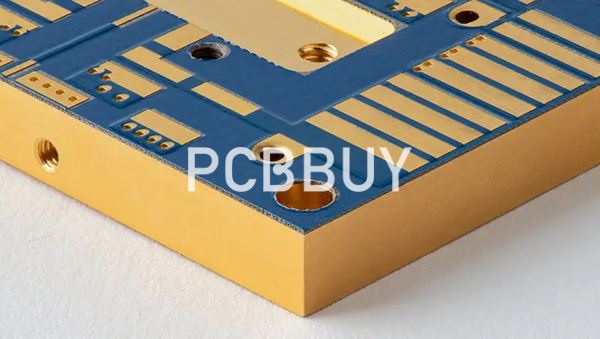
Typical Copper Roughness Levels
Different copper foils are designed for different electrical performance requirements.
|
Copper Type |
Typical Roughness |
Recommended Applications |
|
Standard Copper Foil |
High |
General electronics |
|
Reverse-Treated Copper |
Medium |
High-speed digital circuits |
|
Very Low Profile (VLP) Copper |
Low |
10–25 GHz applications |
|
Ultra Low Profile (ULP) Copper |
Very Low |
High-frequency RF, AI servers, aerospace |
PCB Manufacturing Factors Affecting Surface Roughness
Surface roughness is influenced throughout the PCB fabrication process.
Copper Foil Selection
The base copper foil determines the initial surface profile.
High-speed PCBs often use:
-
VLP copper
-
HVLP copper
-
ULP copper
to reduce conductor loss.
Etching Process Control
Over-etching or uneven etching increases conductor irregularities.
PCBBUY utilizes precision etching technology to maintain:
-
Accurate trace width
-
Smooth conductor edges
-
Consistent copper geometry
Surface Finish Selection
Surface finish also affects conductor performance.
|
Surface Finish |
High-Speed Performance |
|
ENIG |
Excellent flatness and signal performance |
|
ENEPIG |
Excellent for advanced packaging and fine-pitch devices |
|
Immersion Silver |
Excellent conductivity and RF performance |
|
HASL |
Less suitable for very high-speed circuits due to surface unevenness |
PCBBUY supports multiple surface finish options based on customer signal integrity requirements.
PCB Material Selection for High-Speed Applications
Copper roughness works together with dielectric materials to determine total transmission loss.
For high-speed PCB designs, manufacturers typically recommend low-loss laminates.
|
Material Type |
Advantages |
|
Rogers Series |
Low dielectric loss for RF and microwave designs |
|
High-Tg FR-4 |
Improved thermal stability for high-speed digital circuits |
|
Hybrid Stackups |
Balance performance and manufacturing cost |
|
Low-Dk/Low-Df Materials |
Minimize signal attenuation |
PCBBUY supports Rogers, high-Tg FR-4, halogen-free laminates, and mixed-material stackups for high-speed PCB manufacturing.
Manufacturing Technologies That Improve High-Speed Signal Performance
Reliable high-speed PCBs require more than premium materials—they depend on precise manufacturing control.
|
Manufacturing Capability |
Benefit |
|
Controlled Impedance |
Stable signal transmission |
|
Fine-Line Fabrication (35 μm / 1.4 mil) |
Accurate high-density routing |
|
HDI Technology |
Shorter signal paths |
|
Laser Microvias |
Reduced discontinuities |
|
Layer Registration (±25 μm) |
Consistent impedance and routing accuracy |
|
Advanced AOI Inspection |
Detects trace defects before shipment |
These capabilities help maintain electrical consistency throughout prototype and volume production.
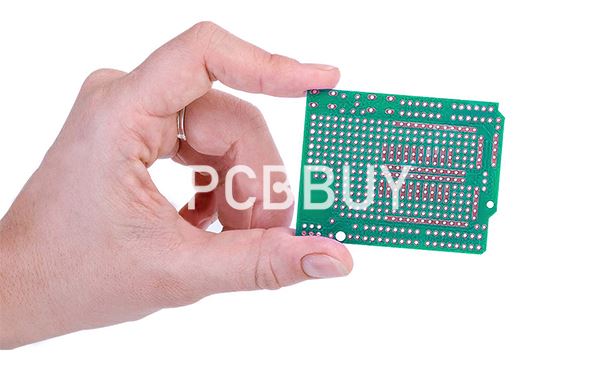
PCBBUY's Manufacturing Advantages for High-Speed PCB Projects
For applications requiring excellent signal integrity, PCBBUY combines advanced fabrication technology with comprehensive quality assurance.
|
PCBBUY Capability |
Customer Benefit |
|
4–26 Layer PCB Manufacturing |
Supports complex networking and computing platforms |
|
HDI PCB Production |
High-density routing for advanced electronic systems |
|
Controlled Impedance Processing |
Consistent electrical characteristics |
|
Fine-Line Technology |
Supports high-speed interfaces and BGA devices |
|
Rogers & High-Speed Materials |
Optimized for RF and microwave applications |
|
AOI, Flying Probe & Electrical Testing |
Ensures manufacturing quality and reliability |
Whether producing prototypes or mass production, PCBBUY helps customers achieve reliable signal performance through strict process control.
Best Practices for Minimizing Surface Roughness Effects
Engineers can reduce conductor-related signal loss by following several design and manufacturing recommendations.
|
Best Practice |
Benefit |
|
Select VLP or ULP copper foil |
Reduces conductor loss |
|
Use low-loss dielectric materials |
Improves signal transmission |
|
Optimize PCB stackup |
Enhances impedance control |
|
Minimize unnecessary via transitions |
Reduces discontinuities |
|
Specify controlled impedance |
Ensures consistent electrical performance |
|
Partner with experienced PCB manufacturers |
Improves production consistency |
Conclusion
As signal frequencies continue to increase, PCB surface roughness effects on high-speed signal become increasingly important in determining overall system performance.
Copper profile influences insertion loss, impedance stability, conductor resistance, and signal integrity, making it a critical consideration for high-speed PCB design and manufacturing.
By combining advanced materials, precision etching, controlled impedance technology, HDI manufacturing, and comprehensive quality inspection, PCBBUY delivers high-performance PCB solutions for networking, AI computing, automotive electronics, RF communication, and other demanding high-speed applications.
FAQ
1. What is PCB surface roughness?
PCB surface roughness refers to the microscopic texture of copper conductors on a printed circuit board. It affects how high-frequency electrical current flows along the conductor surface.
2. Why does surface roughness matter for high-speed signals?
At high frequencies, the skin effect causes current to travel mainly on the conductor surface. Rougher copper increases the current path length and conductor resistance, leading to greater insertion loss and reduced signal integrity.
3. What applications are most affected by copper surface roughness?
Applications include:
-
5G communication equipment
-
AI servers
-
High-speed networking
-
PCIe Gen5/Gen6 systems
-
DDR5 memory interfaces
-
RF and microwave circuits
-
Automotive radar
-
Aerospace electronics
4. Which copper foil is best for high-speed PCB design?
Very Low Profile (VLP), Hyper Very Low Profile (HVLP), and Ultra Low Profile (ULP) copper foils are commonly preferred because they reduce conductor loss while maintaining good adhesion.
5. How does PCB manufacturing influence surface roughness?
Copper foil selection, etching accuracy, chemical treatment, and surface finish all affect the final conductor profile. Tight process control helps maintain consistent electrical performance across production batches.
6. Which surface finish is recommended for high-speed PCBs?
ENIG, ENEPIG, and Immersion Silver are generally preferred for high-speed and high-frequency applications because they provide excellent surface flatness, solderability, and electrical performance.
7. How does PCBBUY support high-speed PCB manufacturing?
PCBBUY offers controlled impedance fabrication, HDI technology, fine-line processing, advanced multilayer manufacturing, Rogers and low-loss material options, precision layer registration, and comprehensive AOI and electrical testing to help customers achieve reliable high-speed PCB performance.
Industry Category








