Carbon Ink PCB Factory and Advanced Carbon Printing Capabilities
By:PCBBUY 07/11/2025 17:06
Why Carbon Ink PCB Technology Matters
In the fast-paced electronics manufacturing world, carbon ink PCB technology plays a crucial role in developing reliable and cost-effective circuit solutions. At PCBBUY, a leading carbon ink PCB factory in China, we offer precision-engineered carbon printing capabilities that support high-performance applications across industries including consumer electronics, automotive systems, remote controllers, and membrane switches.
This article dives into the carbon ink PCB manufacturing process, highlighting our technical specifications, quality benchmarks, and factory strengths that set us apart in the global PCB market.
Understanding Carbon Ink PCBs
Carbon ink is a conductive paste applied to PCB surfaces through screen printing. It is widely used to create keypad contacts, resistors, and jumper connections, offering advantages such as cost reduction and enhanced durability compared to metal plating.
PCBBUY’s Carbon Ink PCB Factory Capabilities
At PCBBUY, we are equipped with high-precision screen printing and curing systems to ensure consistency and performance across every carbon-coated surface. Below are our key carbon ink PCB specifications:
|
Item |
Standard |
Remarks |
|
1. Thickness |
0.4 ± 0.4 mil |
When ≥1 mil is required, secondary printing is needed |
|
2. Surface Width |
Usually >16 mil, min 14 mil |
Less than standard requires review |
|
3. Bridge Width |
Usually >16 mil, min 12 mil |
Less than standard requires review |
|
4. Resistance |
≤50Ω |
Can be customized below 200Ω |
Let’s break down these capabilities in detail:
Carbon Ink Thickness Control
At PCBBUY, we apply carbon ink layers with a standard thickness of 0.4 ± 0.4 mil. If your application requires ≥1 mil, we utilize multi-pass printing with intermediate curing to achieve uniform layering and high adhesion.
This controlled thickness is vital for contact pads used in membrane switches and button pads, ensuring consistent actuation force and electrical conductivity.
Minimum Line Width and Spacing
We support a minimum surface width of 14 mil and a bridge width down to 12 mil, ensuring fine patterning for dense and compact designs. These limits are regularly verified using automated optical inspection (AOI) systems for dimensional accuracy.
If you require finer traces, we can review and evaluate your design on a case-by-case basis for feasibility and quality control.
Stable and Low Carbon Ink Resistance
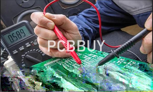
A key metric for performance is carbon trace resistance. Our carbon printing process achieves a maximum resistance of ≤50Ω, suitable for most input circuits and low-current signal paths. For specific applications like low-impedance jumpers or load resistors, we offer customization down to 200Ω or lower.
PCBBUY's Manufacturing Advantages as a Carbon Ink PCB Factory
1. Precision Printing Equipment
We use advanced semi-automatic screen printers with stainless-steel mesh and emulsion frames, delivering accurate carbon paste transfer and repeatability across large panel volumes.
2. Consistent Drying & Curing
Our ovens are calibrated to provide controlled curing temperatures (typically 150°C – 180°C for 30 minutes), ensuring uniform resistivity and mechanical strength across the board.
3. Custom Engineering Review
Our experienced engineering team evaluates all non-standard carbon ink layouts, ensuring that special tolerances, resistance specs, and geometry constraints are met before mass production.
4. Flexible Order Quantities
From prototype batches to mass production, we offer fast turnaround times, competitive pricing, and one-on-one project management—ideal for OEMs, startups, and electronics designers worldwide.

Applications of Carbon Ink PCBs Manufactured by PCBBUY
-
Remote controls: Keypad contact points
-
Membrane switch boards: Conductive button surfaces
-
Touch sensor layers: Alternative to copper contact pads
-
Simple resistors: Fixed resistance paths
-
Jumpers & bridges: Cost-effective short circuits
Why Choose PCBBUY as Your Carbon Ink PCB Factory Partner?
-
✅ In-house screen printing & inspection
-
✅ ISO-certified facilities
-
✅ Experienced engineering support
-
✅ Fast sample delivery & flexible customization
-
✅ Global shipping & multilingual sales team
FAQ: Carbon Ink PCB Factory at a Glance
Q1: What is the typical resistance of PCBBUY’s carbon ink PCBs?
A1: The standard resistance is ≤50Ω, but we can customize values as low as 20Ω depending on the trace design and ink type.
Q2: Can PCBBUY handle multi-layer PCBs with carbon ink printing?
A2: Yes. Carbon ink printing is applied after the top-layer etching process and can be incorporated into single-layer or multi-layer boards.
Q3: Do you offer testing for carbon traces?
A3: Yes. We offer resistance testing, visual inspection, and optional functional pad testing before shipment.
Q4: What industries use your carbon ink PCBs?
A4: Our PCBs are used in consumer electronics, automotive keypads, industrial control panels, and more.
Contact PCBBUY: Your Trusted Carbon Ink PCB Factory in China
At PCBBUY, we combine craftsmanship, innovation, and reliability to provide world-class carbon ink PCB manufacturing services. Whether you're developing a new membrane switch product or looking to optimize your cost structure with carbon printing, we are ready to support your needs.
📩 Contact us today to get a custom quote or engineering review for your carbon ink PCB project!
Industry Category


