Circuit board test method
By:PCBBUY 04/28/2021 11:16

The test is a measurement with experimental nature, that is, a combination of measurement and test. The test means is instrumentation. Because test and measurement are closely related, in actual use, it is often not strict to distinguish between test and measurement. The basic task of the test is to obtain useful information. Through the use of special instruments and equipment, the design of reasonable experimental methods and the necessary signal analysis and data processing, in order to obtain information related to the measured object. The final result of the test is to input the displayed information into the information processing library for control.
Circuit board test process
Detection before power-on: After soldering a circuit board, when checking whether the circuit board can work normally, usually not directly supply power to the circuit board, but follow the steps below to ensure that there is no problem at each step and then power on late:
1. Whether the connection is correct: check whether the board connection is correct according to the schematic diagram, and check one by one according to the circuit diagram of the circuit diagram;
2. Check the installation of the components: whether the diode polar capacitor and the chip are installed correctly. Check whether the soldering of each device has virtual soldering.
3. Check the power supply interface and other short circuits: Check whether there is a short circuit between the power supply and each level. Protection circuits such as resettable fuses should be added to the circuit design. The power supply part can be designed with 0Ω resistance, and the front line of the power supply is not welded to prevent the chip of the back unit from being burned abnormally.
Detection after power on: Check the following steps after power on:、
1. Observation of power-on: Do not rush to measure electrical indicators after power-on, but observe whether the circuit has abnormal phenomena, such as smoke, abnormal smell, touch the outer package of the integrated circuit, whether it is hot, etc. If an abnormal phenomenon occurs, turn off the power supply immediately, and then check the power supply after troubleshooting.
2. Static test: Check whether the level status reaches the expectation step by step, and gradually restore the welding 0Ω resistance. The debugging sequence of the sub-circuit is generally carried out according to the signal flow direction, and the output signal of the circuit that has been debugged before is used as the input signal of the subsequent stage to create conditions for the final unified adjustment.
3. Dynamic test: gradually add external input and output signals to debug various parts of the system. This step requires joint debugging with software.
Test method of circuit board
1. Manual visual inspection:
Use a magnifying glass or calibrated bai microscope, and use the visual inspection of the operator to confirm that the circuit board is unqualified and determine when correction operation is required. It is the most traditional and the most important detection method. Its main advantages are low upfront costs and no test fixtures, and its main disadvantages are human subjective errors, high long-term costs, discontinuous defect detection, and difficulty in data collection. At present, due to the increase in the output of PCBs and the reduction in the spacing of wires on the PCB and the volume of components, this method has become less and less feasible.
2. Online testing (ICT, In Ciruit Testing)
ICT finds manufacturing defects and tests analog, digital and mixed-signal components through the inspection of electrical performance to ensure that they meet specifications. There are Bed of Nails Tester and Flying Probe Tester ) Wait for several test methods. The main advantages of ICT are low test cost per board, strong digital and functional test capabilities, fast and thorough short-circuit and open-circuit testing, programming firmware, high defect coverage, and easy programming. The main disadvantages are the need for test fixtures, programming and debugging time, the high cost of making fixtures, and the difficulty of using them
3. Functional Testing
The functional system test is to use special test equipment at the middle and end of the production line to comprehensively test the functional modules of the circuit board to confirm the quality of the circuit board. Functional testing can be said to be the earliest automatic testing principle. It is based on a specific board or a specific unit and can be completed with various devices. There are final product test (Final Product Test), the latest solid model (Hot Mock-up) and "stacked" test ('Rack and Stack' Test) and other types. Functional testing usually does not provide footsteps for process improvement and Deep-level data such as component-level diagnostics, and requires special equipment and a specially designed test process to write functions
The test procedure can be complicated, so it is not suitable for most circuit board production lines.
4. Automatic optical detection
Also known as automatic visual inspection, it is based on the principle of optics, using a variety of technologies such as image analysis, computer and automatic control to detect and process defects encountered in production, which is a relatively new method of confirming manufacturing defects. AOI is usually used before and after reflow and before electrical testing to improve the pass rate in the electrical processing or functional testing phase. At this time, the cost of correcting defects is much lower than the cost of conducting after the final test, often reaching a dozen times.
5. Automatic X-ray Inspection (AXI, Automatic X-ray Inspection)
AXI makes use of the difference in X-ray absorption rate of different substances to see through the parts to be detected and find defects. It is mainly used to detect defects such as ultra-fine pitch and ultra-high-density circuit boards and bridging, chip dropping, and misalignment during the assembly process. It can also use its tomography technology to detect internal defects in IC chips. It is currently the only way to test the soldering quality and blocked solder balls of Ball Grid Array (BGA). In the latest AXI system for circuit board assembly, the latest products of companies such as Feinfocus, Phoenix Xray, etc. can not only perform 2D perspective inspection, but also provide 3D inspection through the sample side tilt, "side-view" X-ray information. Its main advantages are the ability to detect BGA welding quality and embedded components, and no fixture cost; the main disadvantages are slow speed, high failure rate, difficulty in detecting reworked solder joints, high cost, and long program development time.
6. Laser detection system
It is the latest development of PCB testing technology. It uses a laser beam to scan the printed board, collect all measurement data, and compare the actual measurement value with the preset qualified limit value. This technology has been confirmed on the light board, and is being considered for assembly board testing, and the speed is sufficient for mass production lines. Fast output, without requiring fixtures and visual uncovered access are its main advantages; high initial cost, and maintenance and use problems are its main disadvantages.
From the above 6 commonly used PCB inspection methods, it can be found that AOI automatic optical inspection equipment, like any vision-based inspection system, can only detect faults that can be seen with vision, and can only detect defects such as short circuits and open circuits. Use electrical test method to solve. Compared with the primitive visual detection method of human naked eye, AOI is an automated detection method, and its detection efficiency is much higher and its reliability is much more stable.
7. Needle bed method
This method bai is connected to each detection point on the electric circuit board by a probe with a spring. The spring makes each probe have a pressure of 100-200g, to ensure that each detection point is in good contact, such a probe is arranged together is called a "needle bed". Under the control of the inspection software, the inspection points and inspection signals can be programmed, and the inspector can get the information of all the inspection points.
In fact, only those probes that need to be tested are installed. Although the needle bed test method may be used to test both sides of the circuit board at the same time, when designing the circuit board, all the detection points should be on the soldering surface of the circuit board. Needle bed tester equipment is expensive and difficult to maintain. The needles are selected in different arrangements according to their specific application.
A basic general-purpose grid processor consists of a drilled board with a pin center spacing of 100, 75, or 50 mils. Pins act as probes and make direct mechanical connections using electrical connectors or nodes on the circuit board. If the pads on the circuit board match the test grid, a vinegar film that is perforated according to the specifications will be placed between the grid and the circuit board to facilitate the design of specific probes.
Continuity detection is achieved by accessing the end point of the grid (which has been defined as the x-y coordinate of the pad). Since every network on the circuit board is tested for continuity. In this way, an independent test is completed. However, the proximity of the probe limits the effectiveness of the needle bed test.
8.Observation
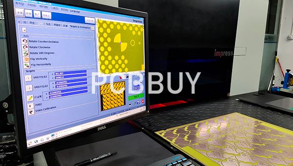
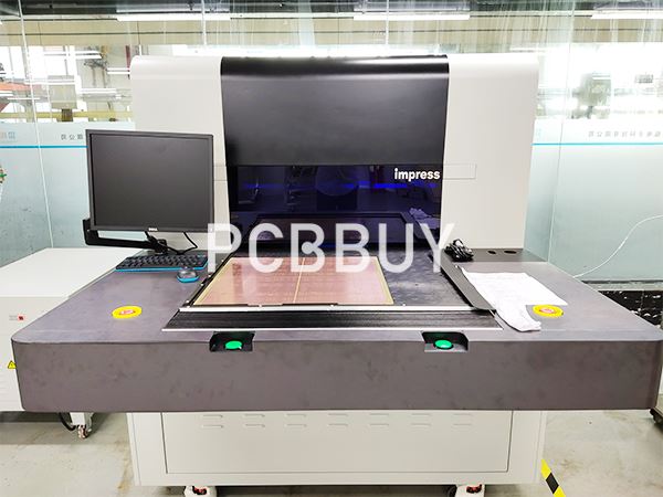
The circuit board is small in size and complex in structure, so professional observation instruments must also be used to observe the circuit board. In general, we use a portable video microscope to observe the structure of the circuit board. Through the video microscope camera, you can clearly see the microstructure of the circuit board from the microscope. In this way, it is easier to design and test the circuit board.
9. Flying probe test
The flying probe tester does not depend on the pin pattern installed on the fixture or bracket. Based on this system, two or more probes are mounted on a tiny magnetic head that can move freely on the x-y plane, and the test points are directly controlled by CADI Gerber data. The dual probes can move within 4mil of each other. The probes can move independently, and there is no real limit to how close they are to each other.
The tester with two arms that can move back and forth is based on the measurement of capacitance. The circuit board is pressed tightly on the insulating layer of a metal plate, which is used as another metal plate of the capacitor. If there is a short circuit between the lines, the capacitance will be larger than at a certain point. If there is an open circuit, the capacitance will become smaller.
Industry Category


