Comprehensive Guide to PCBA DFM
By:PCBBUY 10/20/2025 15:34
Why PCBA DFM Matters in Modern Electronics
The perception of design in the ever-changing manufacturing of electronics is not about creativity any longer, but about manufacturability. PCBA DFM (Design for Manufacturability) is an imperative which helps fill the gap between the circuit design and the actual PCB production. An excellent schematic may fail because it has not been designed to be assembled, soldered or tested.
At PCBBUY, we apply DFM throughout all phases of the production process - when examining a design file, assembling a prototype, and so on - so that any board to leave this plant will be not only accurate by engineering standards but also economical to manufacture.
What Is PCBA DFM and Why It’s Critical
PCBA DFM is the systematic evaluation of your PCB design to ensure it can be manufactured efficiently, reliably, and at scale. It focuses on identifying potential production issues before they become costly problems.
This includes checking for:
-
Component spacing and placement accuracy
-
Pad and hole alignment for solderability
-
Copper-to-edge clearance and trace width uniformity
-
Thermal relief and impedance control
-
Stencil design and solder paste volume optimization
By performing these checks early, PCBBUY’s engineering team ensures that each design moves smoothly from digital layout to physical board — reducing rework, delays, and yield loss.
How PCBBUY’s PCBA DFM Process Works
PCBBUY has a well-organized DFM review workflow that integrates automation, expertise, and precision engineering.
1. Pre-Check and File Submission
As you submit your Gerber, BOM or pick-and-place files, a verification of initial DFM is automatically done by our system. Some of the typical design risks that are scanned by the automated tool include solder mask openings, drill to copper violations or lack of alignment of the silkscreen.
2. Engineering Review
Then manually read by our senior CAM (Computer-Aided Manufacturing) engineers. They assess aspects like:
Aspect ratios of through holes on plated through holes.
• High-speed signal routing controlled impedance.
• Copper balancing to prevent balancing in reflowing of boards.
Every project is given a specific DFM engineer and he/she is given detailed feedback prior to the onset of production.

3. Feedback and Optimization of the customers
After the DFM results have been summarized, PCBBUY provides a report displaying suggested areas of improvement, such as the recommendation to increase pad size to optimize solder joints or move vias around BGAs to increase yield. This prevention policy provides the customers with the visibility and control of the fabrication.
4. Production Validation
Once the design passes approval, pilot run is done on our in-house SNT and assembly lines. The process includes:
• Checking the stencil alignment.
• Reflow profile calibration
• BGA and fine-pitch component optical and X-ray inspection.
Full-scale production does not begin until then, when it is validated, which means that there are no surprises at all when producing in large quantities.
Key Benefits of PCBA DFM at PCBBUY
Implementing a strong PCBA DFM process doesn’t just prevent defects — it transforms the entire production flow.
|
Benefit |
Description |
|
Higher Yield |
Optimized design parameters minimize solder bridges, tombstoning, and cold joints. |
|
Shorter Lead Time |
Early detection of design flaws avoids costly revisions mid-production. |
|
Lower Costs |
Less rework, scrap, and wasted material. |
|
Improved Reliability |
Stable mechanical and electrical performance under diverse conditions. |
|
Better Scalability |
Seamless transition from prototype to full production runs. |
At PCBBUY, we treat DFM not as a one-time check but as a continuous collaboration between our engineers and your design team.
Real-World Example: DFM in Action
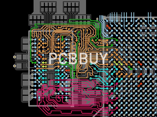
One of our customers has presented 10 layers PCB HDI design with dense BGA routing. In the process of DFM review, our engineers had identified possible bridging of solder under a few 0.4mm pitch BGAs.
Following a simple design fix and a slight adjustment of the solder, solder faults decreased by 92% on the initial batch. This active DFM move saved time of reassembly and cost of components.
A normal outcome of such a DFM check by PCBBUY hands-on method - each board is treated as though it were our own.
How to Get a Free DFM Review with PCBBUY
PCBBUY offers free PCBA DFM evaluation for all uploaded Gerber and BOM files before production begins.
Simply visit our online quote system, upload your files, and our engineers will return a full DFM report within hours. This ensures your design is ready for smooth manufacturing, even before you place your order.
Conclusion
PCBA DFM must not be an after thought, whether you are creating a prototype or large scale mass production.
We understand that manufacturability is the secret of long-term reliability at PCBBUY, and that is what we have created our whole production system. Since early design checking till the finer SMT assembly, PCBBUY promises too have all the circuit boards built on the first attempt.
FAQ: Common Questions About PCBA DFM
1️⃣ What does DFM mean in PCBA manufacturing?
DFM (Design for Manufacturability) refers to the process of evaluating and improving PCB layouts to make them easier, cheaper, and more reliable to manufacture and assemble.
2️⃣ How does PCBBUY perform DFM checks?
Our system uses automated DFM analysis combined with expert engineer review. Each design is checked for spacing, solder mask alignment, copper balancing, and more — all before production begins.
3️⃣ Why should I request a DFM review before production?
A DFM review ensures your design is optimized for real-world production, which helps reduce soldering defects, improve yield, and save both time and cost in the long run.
Industry Category


