Comprehensive Overview of PCB Engineering Process
By:PCB 01/23/2024 09:43

The PCB engineering process is a complex series of steps involving multiple stages and techniques to ensure that the final Printed Circuit Board (PCB) meets design requirements and performance standards. The following is a comprehensive overview of the entire PCB engineering process, covering the entire workflow from design to testing.
PCB Design
The starting point of the PCB engineering process is the design phase. In this stage, engineers transform circuit schematics into PCB layouts. This process includes the following steps:
Determine PCB Size and Shape: Choose appropriate PCB size and shape based on circuit requirements and expected component count.
Layout Planning: Determine the positions of components on the PCB to meet electrical, mechanical, and manufacturability requirements.
Define Routing Rules: Set parameters such as signal line width and spacing to ensure proper electrical connections and signal integrity.
Create Layers: Based on circuit requirements, divide the PCB into multiple layers, including signal layers, power layers, and ground layers.
Generate Design Data: Use Electronic Design Automation (EDA) tools to export design data as manufacturing files for subsequent PCB fabrication.

PCB Formation
After completing the design, the PCB enters the formation stage. This stage includes the following steps:
Drilling: Drill holes in the PCB according to design data for component installation and electrical connections between different layers.
Graphic Cutting: Use laser or mechanical cutting methods to follow the designed circuit paths and cut out the outlines of the traces.
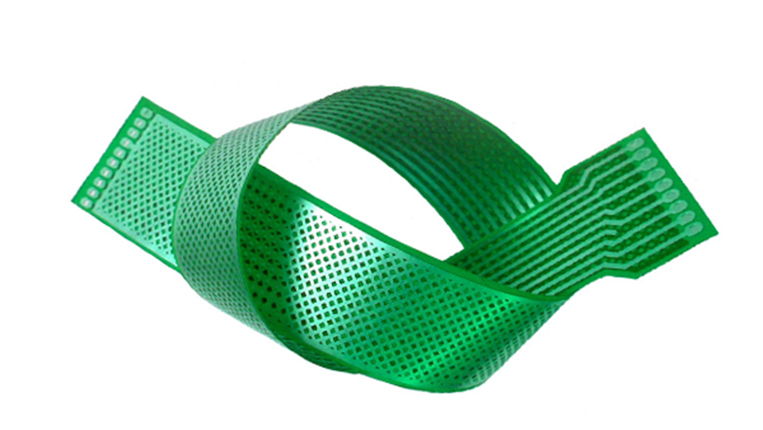
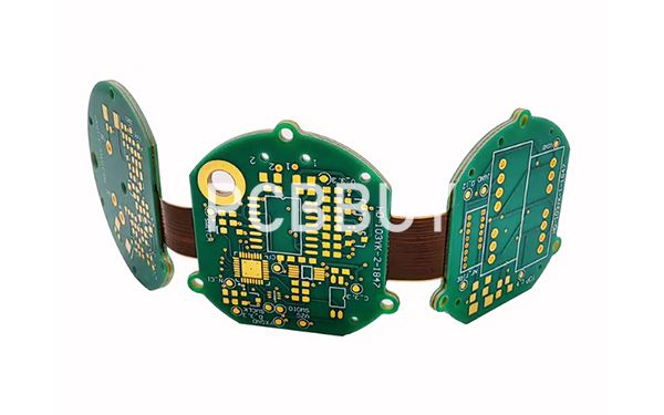
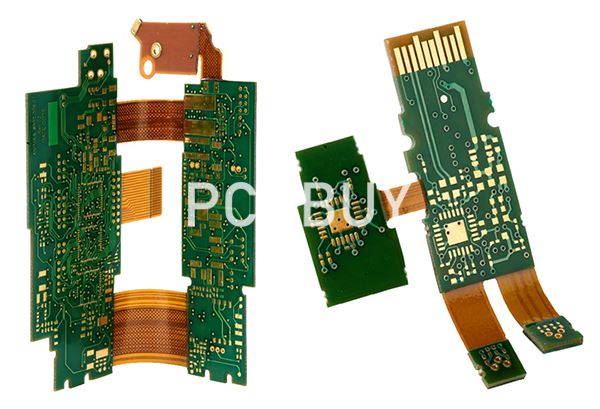
Shaping and Lamination: Bend, fold, or press the PCB according to design requirements and laminate multiple layers together to achieve the desired electrical performance and mechanical strength.
Surface Treatment
Surface treatment is a crucial step to ensure good solderability and corrosion resistance of the PCB. Common surface treatment methods include:
Chemical Nickel Gold Plating: Deposit a layer of nickel-gold alloy on the copper foil surface using a chemical process to improve conductivity and corrosion resistance.
Hot Air Leveling: Use high-temperature airflow to blow molten solder onto the copper foil surface, forming a metallic layer to enhance solderability and corrosion resistance.
Organic Coating: Apply a layer of organic insulation material on the copper foil surface to protect it from environmental factors and mechanical damage.
Component Installation
Component installation is one of the most complex stages in the PCB manufacturing process. Depending on the component type and installation process, it can be divided into several methods:
Surface Mount Technology (SMT): Suitable for the installation of small components like chips, capacitors, resistors, etc. Components are attached to the soldering surface of the PCB using soldering techniques.
Through-Hole Technology (PTH): Suitable for the installation of larger components such as IC chips and transistors. Components are inserted into drilled holes in the PCB and soldered in place.
Press-Fit Technology: Suitable for high-mechanical-strength connections, such as connectors and terminals. Conductors are pressed onto the PCB surface using specially designed connectors.

Soldering Techniques
Soldering is the process of connecting components to the PCB. Common soldering techniques include:
Manual Soldering: Use tools like soldering irons to melt solder and attach components to the PCB. Suitable for small-scale production and repairs.
Wave Soldering: Immerse the PCB in molten solder using a wave motion, ensuring even application of solder over the PCB surface. Suitable for large-scale production.
Reflow Soldering: Melt solder by heating, allowing it to reflow and bond components to the PCB. Suitable for surface-mount components.
Testing Techniques
Testing is a crucial step to ensure PCB performance and quality. Common testing methods include:
Visual Inspection: Examine the PCB visually or under a microscope to check for defects or errors in traces and component installation.
In-Circuit Testing (ICT): Use test probes to detect connectivity and assess the quality of solder joints at each node on the PCB.
Functional Testing: Test the functionality of the PCB by installing it on a test fixture and verifying if it meets design requirements and performance standards.
Load Testing: Subject the PCB to electrical tests simulating real-world conditions to assess its performance and reliability.
Environmental Testing: Expose the PCB to extreme conditions such as high/low temperatures and humidity to evaluate its adaptability and reliability.
Electromagnetic Compatibility (EMC) Testing: Assess the PCB's electromagnetic radiation and interference resistance against relevant standards and specifications.
Reliability Testing: Evaluate the PCB's lifespan and reliability through accelerated aging, endurance tests, etc.
Fault Diagnosis and Repair: Diagnose and repair any issues identified during testing to enhance the product's yield and reliability.
Industry Category


