Controlled Depth Back Drilling for Via Stub Minimization in High-Speed PCBs
By:PCBBUY 10/27/2026 15:02

Introduction
As high-speed interfaces become more common in automotive electronics, industrial control systems, power equipment, and energy-storage products, PCB via design plays an increasingly important role in signal integrity. A conventional plated through-hole via may extend through several layers even when the signal uses only part of the barrel. The unused section, known as a via stub, can create impedance discontinuities, reflections, and unwanted resonances.
Controlled depth back drilling for via stub minimization removes most of the unused plated barrel while preserving the electrical connections required by the design. Its effectiveness depends on accurate stack-up planning, drilling-depth control, registration, and clear communication between the PCB designer and manufacturer.

1. What Is Controlled-Depth Back Drilling?
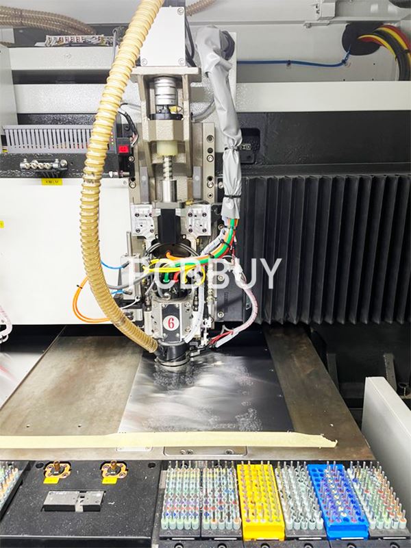
Back drilling is a secondary mechanical drilling process performed after through-hole plating. A drill with a larger diameter than the original plated via removes the unwanted copper barrel from the selected side of the PCB. The process stops before reaching the functional layer that must remain connected.
The goal is not necessarily to eliminate every part of the stub. Instead, the remaining stub should meet the electrical design target while maintaining sufficient manufacturing margin to protect functional copper.
Long via stubs can behave as unwanted transmission-line branches. Depending on signal frequency, rise time, stub length, and stack-up, they may contribute to reflections and resonance that degrade channel performance. Back drilling is therefore often considered for high-speed multilayer boards where through-hole vias are needed but unused barrel length must be reduced.
2. Key Design and Manufacturing Parameters
Successful back drilling requires the design team to define more than a nominal drilling depth. The drill entry side, target layer, residual stub limit, back-drill diameter, and copper clearance must be reviewed together.
|
Parameter |
Engineering consideration |
|
Back-drill entry side |
Identify whether drilling is performed from the top, bottom, or both sides. |
|
Target and protected layers |
Specify the layer where the back drill should stop and the copper that must not be damaged. |
|
Residual stub length |
Set the maximum allowable remaining stub based on signal-integrity analysis and confirmed manufacturing capability. |
|
Back-drill diameter |
Select a suitable diameter to remove the unused barrel while maintaining clearance from nearby copper features. |
|
Stack-up and dielectric thickness |
Confirm that the planned drilling depth leaves adequate margin to the protected layer. |
|
Registration and depth control |
Account for drilling variation, layer alignment, board thickness variation, and the selected manufacturing process. |
A critical distinction is that drilling-depth tolerance and residual-stub tolerance are related but not identical. The final stub length also depends on the actual layer position, dielectric thickness, board thickness, and the reference used to define the drill depth. A universal tolerance should not be assumed for every PCB design.
3. How to Optimize Back Drilling for Via Stub Minimization
Define the Requirement During Stack-Up Design
Back drilling should be planned before fabrication data is finalized. Designers should identify the signal layers, via transitions, drill entry side, target layer, and maximum residual stub length. If the requirement is introduced only after the stack-up is fixed, available drilling depth and clearance may limit the achievable result.
For high-speed differential pairs, evaluate both signal vias together. Symmetrical transitions, suitable ground-via placement, and a continuous return-current path help prevent the back-drilled structure from becoming only a partial solution to the signal-integrity problem.
Check Clearance for the Larger Drill
Because the back-drill bit is larger than the original via, the design must provide enough clearance through the layers traversed by the drill. Anti-pad dimensions and nearby copper features should be checked against the actual back-drill diameter, not just the original plated-hole size.
Designers should also verify that the back-drill operation will not remove copper needed by another net or sever a required connection. Manufacturing data should clearly identify the vias to be back drilled and the layers that must remain intact.
Validate the Process with the Manufacturer
The appropriate process window depends on the PCB thickness, layer count, material construction, via geometry, drilling direction, and residual-stub requirement. Before production, the manufacturer should review the stack-up and drill files and confirm achievable depth control, registration, clearance, and inspection methods for the specific design.
Back drilling is not always the best or most economical solution. Depending on the routing density and electrical target, blind vias, buried vias, HDI microvias, or a revised stack-up may provide a better balance between signal integrity, manufacturability, and cost.

4. PCBBUY and PCBBUY Engineering Support
For customers in automotive electronics, industrial control, power and electrical systems, power supplies, energy storage, new energy, and embodied robotics, PCBBUY can help coordinate design requirements with PCBBUY's PCB manufacturing review.
PCBBUY's relevant manufacturing capabilities include multilayer PCB production, HDI structures, fine-line fabrication, controlled registration, and support for high-speed or high-frequency laminate options. Its stated general capabilities include boards up to 26 layers, minimum line width down to 35 μm (1.4 mil), and HDI processing. These general capabilities provide useful context for complex designs, but they do not by themselves guarantee a particular back-drill depth tolerance or residual-stub length.
For projects requiring controlled-depth back drilling, the engineering review should confirm the following before order release:
-
Gerber or ODB++ data, drill files, and the complete layer stack-up.
-
Back-drill side, diameter, target layer, and protected layer.
-
Maximum residual stub length and applicable depth tolerance.
-
Copper and anti-pad clearance along the back-drill path.
-
Inspection and verification requirements agreed for the specific order.
PCBBUY also uses inspection and electrical-testing methods such as AOI, flying-probe testing, and four-wire low-resistance testing where applicable. These methods support manufacturing quality control, but they do not independently prove the residual stub length. If direct confirmation of the back-drilled geometry is required, the inspection plan should specify a suitable method—such as an agreed cross-section or other validated verification procedure—before production begins.
5. Quality Control and Shipment Acceptance
A reliable back-drilled PCB should be assessed against the approved fabrication drawing, drill data, stack-up, and purchase specifications. Acceptance criteria should cover both the back-drill geometry and the board's electrical requirements.
|
Quality item |
Recommended acceptance basis |
|
Back-drill location and diameter |
Match the approved drill data and drawing tolerances. |
|
Drilling depth and residual stub |
Meet the project-specific limits confirmed by the manufacturer before production. |
|
Protected-layer integrity |
No unacceptable damage to functional pads, copper planes, or required connections. |
|
Electrical continuity and isolation |
Pass the applicable electrical test requirements. |
|
Signal-integrity performance |
Meet the project's defined impedance and channel-performance targets when such testing is specified. |
|
Shipment documentation |
Provide agreed inspection records and test reports where required by the purchase specification. |
There is no single residual-stub limit or depth tolerance suitable for every high-speed PCB. For demanding automotive, industrial, and energy applications, the customer and manufacturer should agree on the applicable drawings, acceptance limits, and evidence of compliance before mass production.

Conclusion
Controlled depth back drilling for via stub minimization is an effective option for reducing the electrical impact of unused plated-through via barrels in high-speed multilayer PCBs. Its success depends on coordinated stack-up design, drill-depth control, adequate copper clearance, and verification against project-specific requirements.
By involving PCBBUY and PCBBUY engineering early, customers can evaluate back drilling alongside HDI and alternative via structures, clarify manufacturing limits, and establish practical inspection and shipment criteria before production begins.
FAQ
1. Why is controlled-depth back drilling used in high-speed PCBs?
It removes most of the unused plated barrel in a through-hole via, reducing the potential for reflections, resonance, and impedance discontinuities caused by a long via stub.
2. Does back drilling completely eliminate a via stub?
Not necessarily. A short residual stub is commonly left to protect the functional connection and avoid damaging the target layer. The allowable residual length should be defined by signal-integrity requirements and confirmed manufacturing capability.
3. What information should be provided for a back-drilled PCB quotation?
Provide the complete stack-up, Gerber or ODB++ files, plated-hole and back-drill files, drill entry side, target and protected layers, required residual stub length, and any special inspection criteria.
4. Can PCBBUY guarantee the same back-drill tolerance for every board?
No universal tolerance should be assumed. The achievable tolerance depends on the board construction and drilling requirements. PCBBUY should review the specific design and confirm the applicable process capability before the order is released.
5. Is back drilling necessary for every high-speed PCB?
No. The need depends on signal frequency content, channel performance, via geometry, stack-up, and cost targets. A design review may recommend back drilling, HDI vias, a revised stack-up, or a combination of approaches.
Industry Category